Nanoscratch Testing: An Overview
Analyzing Thin Films and Bulk Materials with Nanoscratch Testing
Nanoscratch testing is a versatile tool for analysis of both thin films and bulk materials. Nanoscratch testing provides the capability to investigate modes of deformation and fracture that are not possible using standard indentation techniques.
Contents include:
KEYWORDS: Nanomechanical Testing; Hysitron; Bruker; Tecnical Note; TN1501; TriboScan; Nanoscratch; SPM Imaging
How Nanoscratch Testing Works
Nanoscratching is accomplished by applying a normal load in a controlled fashion while measuring the force required to move the tip laterally across the sample. By selecting the appropriate normal loading profile and lateral displacement pattern, many different types of tests can be performed. The damage incurred from the test is then typically observed using optical or Scanning Probe Microscopy (SPM) imaging. Bruker’s Hysitron® nanoindenters provide in-situ SPM imaging of the sample with nanometer resolution for immediate feedback of the test results.
Easily Acquire Quantitative Results
Nanoscratch can be used for a wide range of different tests and comes with a versatile load function editor for simple test design. Bruker has created TriboScan™, an easy-to-use software product, designed by experimentalists for experimentalists.
This software allows the user to define the applied normal load and the lateral displacement across the surface of the sample. A single scratch with a ramped normal load is shown in Figure 1. From this data, useful information such as critical load, film adhesion, and delamination force can be measured. The software can also be used to generate a load function that repeatedly scratches over the surface of the sample with a defined normal load, thus enabling reciprocating wear testing. Nanoscratch data, in conjunction with in-situ SPM images, provides a wealth of information concerning a material’s behavior under simultaneous normal and lateral stresses.
Nanoscratch Analysis Software
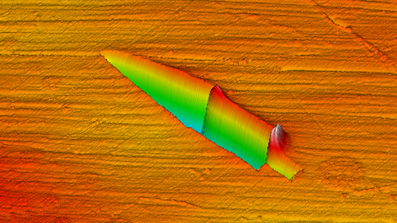
In addition to TriboScan software for test setup and analysis, Bruker’s Hysitron nanoscratch systems come standard with TriboView™, an offline analysis package that enables users to gain additional information from images generated using in-situ SPM imaging (see Figure 2). Users can also use TriboView to quickly generate images and plots for reporting purposes, including 3D images (see Figure 3).
Hysitron, TriboScan, and TriboView are trademarks of Bruker Corporation. All other trademarks are the property of their respective companies. © 2018 Bruker Corporation. All rights reserved. TN1501, RevA0.

