
Over 15 Years of Advancing Scientific Research with PeakForce Tapping Modes
Expand sample compatibility and access material properties
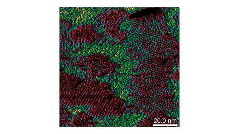
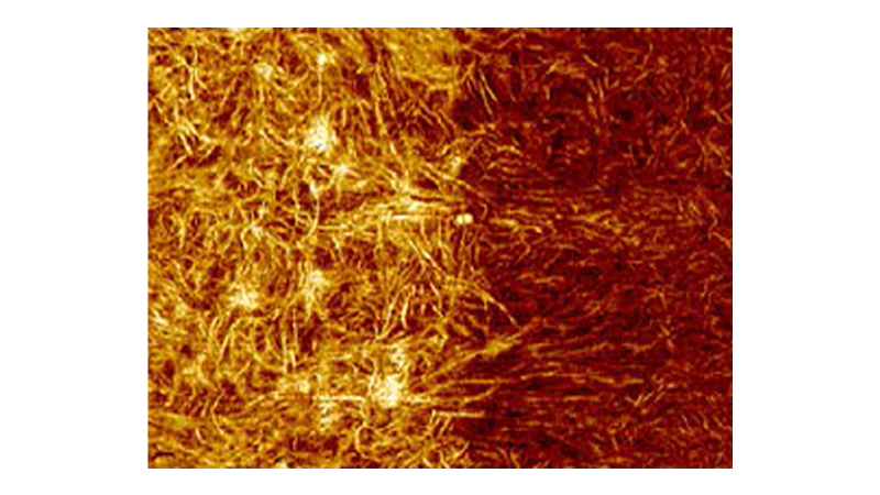
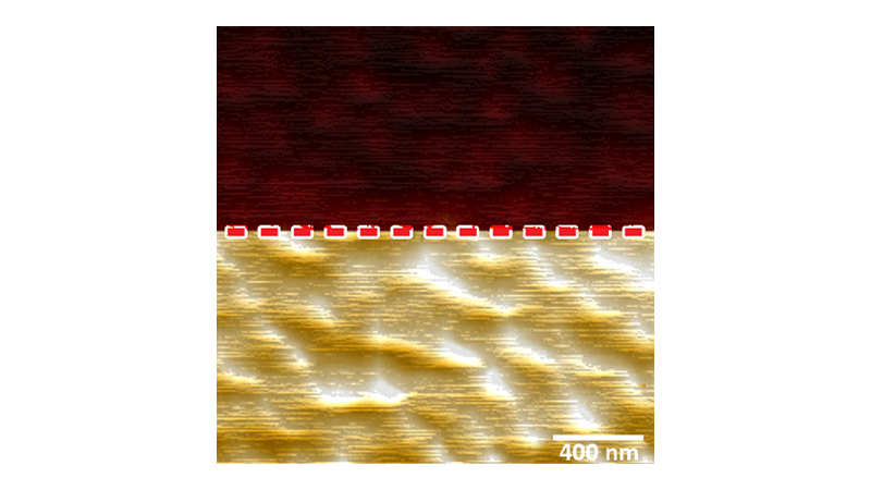
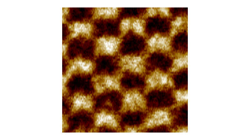
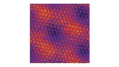
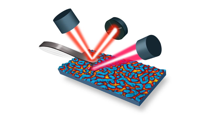
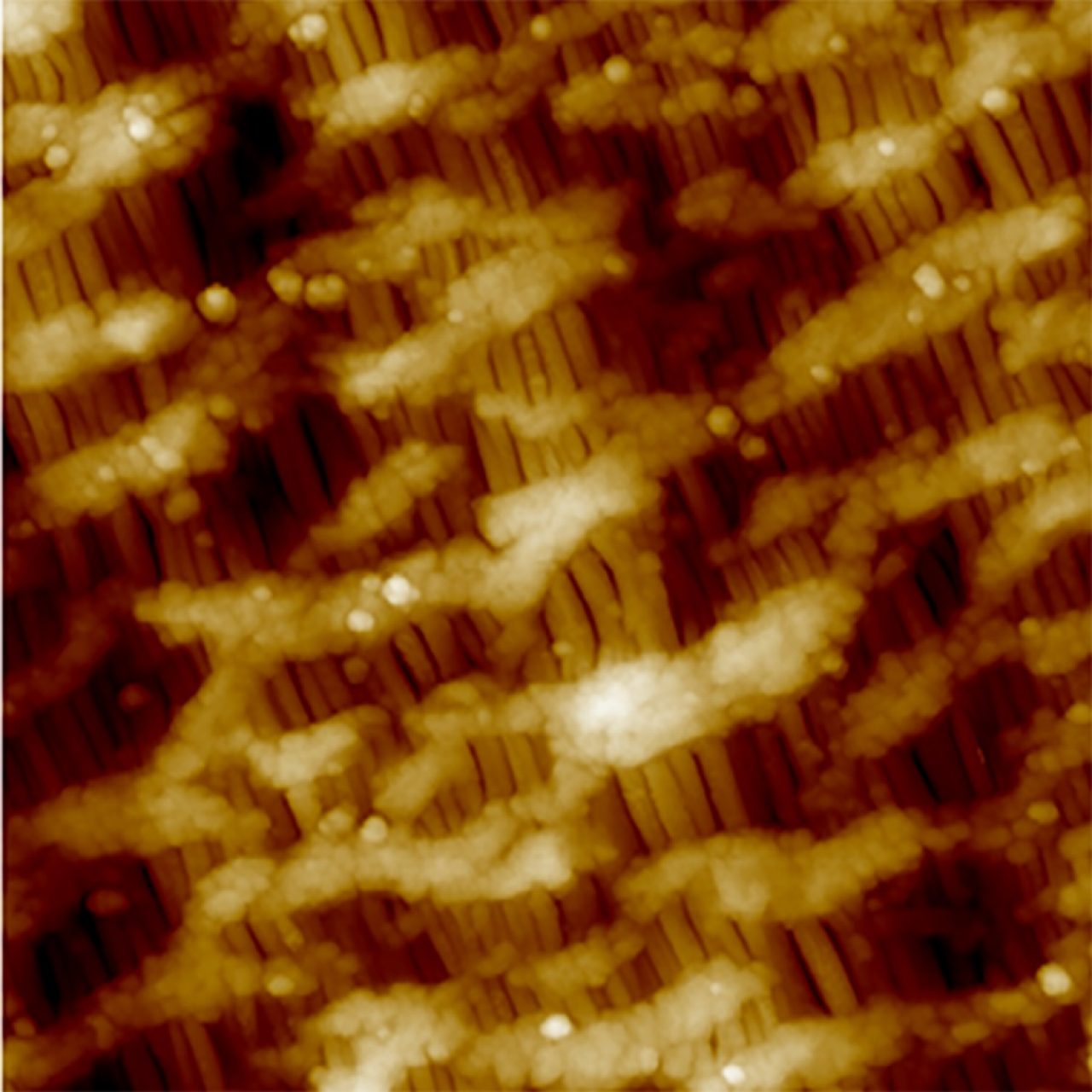
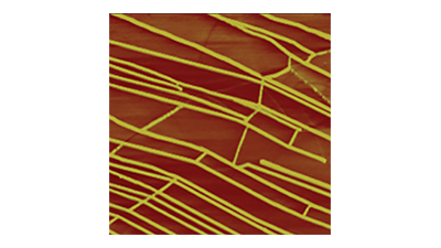
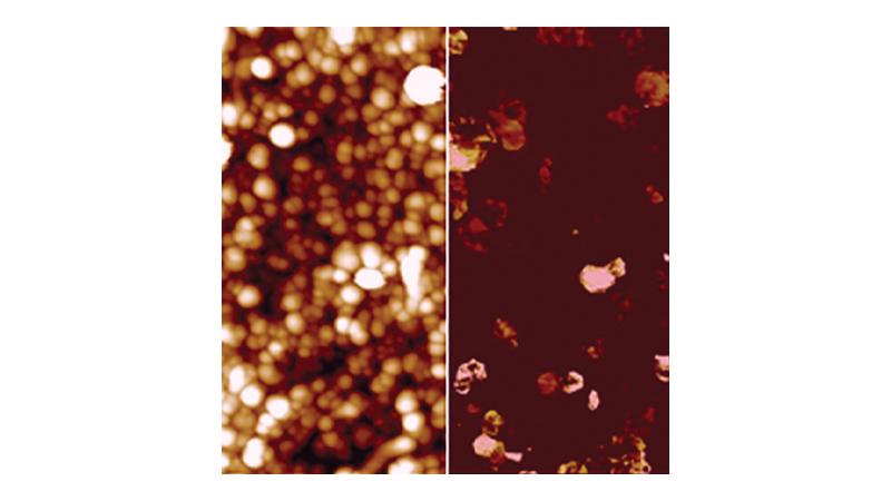
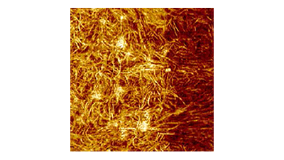
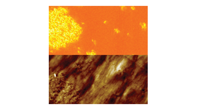
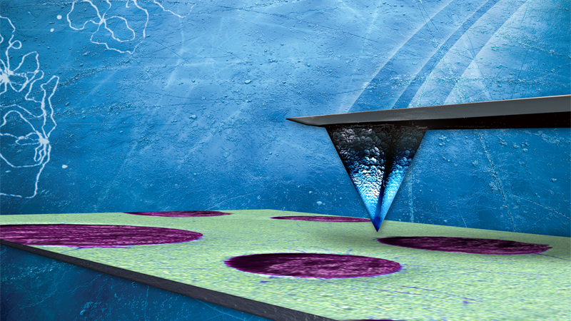
Bruker’s PeakForce Tapping technology provides unprecedented high-resolution imaging, extends AFM measurements into a range of samples not previously accessed, and uniquely enables simultaneous nanoscale property mapping.
Over the last 15 years, the use of PeakForce Tapping has expanded and evolved to span a broad range of research fields. There are now numerous associated modes and capabilities, and it can be found cited in ~10,000 peer-reviewed publications since its inception.
With a technology so powerful and versatile, there is an obvious question to be asked: What is your favorite PeakForce Tapping mode?
We ask our experts for their answers.
Watch this on-demand webinar to:
- Learn what makes PeakForce Tapping so significant
- Meet Bruker application scientists from around the world
- Discover interesting new ways to use this technology
PeakForce Tapping Trivia
Bruker introduced PeakForce Tapping in December of 2009, and its use and applications have been expanding ever since. It has outpaced all other recently developed AFM mode technologies in terms of research impact and productivity.
There are currently at least seven related modes (see our AFM Modes Handbook for more details on those), but users also create their own sometimes, so you tell us!
PeakForce Tapping is an operating mode and ScanAsyst is an automatic image optimization software. Bruker designed the original ScanAsyst to optimize PeakForce Tapping scans only, so the two were sometimes used interchangeably. Now, however, ScanAsyst Plus can be used to optimize any topography scan, whether you’re working in contact mode, TappingMode, or PeakForce Tapping
Summary
No abstracts
Find out more about the technology featured in this webinar or our other AFM Modes:


Bruker Speakers

Peter De Wolf, Ph.D., Director of Technology & Application Development
Peter De Wolf is director for AFM technology & application development at Bruker Nano Surfaces, covering all applications related to Scanning Probe Microscopy (SPM). He obtained his PhD from IMEC, Belgium on the development of new SPM methods for 2D carrier profiling in semiconductors and has more than 25 years of experience on SPM. He is the author and co-author of over 30 publications related to electrical characterization using SPM. He also owns several SPM patents, and developed several new SPM modes for electrical characterization.

Ian Armstrong, Ph.D., Senior Manager AFM Probes, Bruker
Ian Armstrong has worked at Bruker for over 16 years in various roles from applications to product management. He is currently senior manager of Bruker's AFM probes business unit.
Bede Pittenger, Ph.D., Sr. Staff Development Scientist, AFM Applications, Bruker Nano Surfaces
Dr. Bede Pittenger is a Senior Staff Development Scientist in the AFM Unit of Bruker's Nano Surfaces Business. He received his PhD in Physics from the University of Washington (Seattle, WA) in 2000, but has worked with scanning probe microscopes for 25 years, building systems, developing techniques, and studying properties of materials at the nanoscale. His work includes more than thirty publications and three patents on various techniques and applications of scanning probe microscopy. Dr. Pittenger's interests span topics from interfacial melting of ice, to mechanobiology of cells and tissues, to the nanomechanics of polymers and composites.
Khaled Kaja, Ph.D., Applications Scientist
Dr. Khaled Kaja holds a PhD in Nanophysics from the University of Grenoble. He started his research journey at the Leti laboratory (French commission of atomic and alternative energies, CEA) working on the development of highly-resolved nanoelectrical AFM measurements. Following a post-doctoral training at the Swiss federal institute (ETH) Zurich under the chair of nanotechnology (Prof. Dr. Andreas Stemmer), he moved to the UK joining Bruker nano surfaces as an applications scientist. In 2017, Dr. Kaja moved to the middle east as an assistant professor of physics at different universities in the region. Later in 2020, he joined the French national metrology lab (LNE) as a research scientist working on the development of nanoelectrical metrology. Recently, Dr. Kaja joined Bruker nano surfaces and metrology in Karlsruhe (Germany) as an applications scientist. His main research interests are focused on the development of novel nanoelectrical AFM methods applied to 2D materials and low dimensional systems.

Senli Guo, Ph.D., NA Applications Manager, Bruker
Senli earned his Ph.D. in physical chemistry from Duke University (2009) and spent two years in the Center for Nanophase Materials Sciences (CNMS) at Oak Ridge National Lab as a postdoc before joining Bruker as an applications scientist in 2011. All of Senli’s research is about AFM-based methodology developments to address various nanoscience research, ranging from single-molecule interactions to lithium-ion battery electrode properties.

John Thornton,
Senior Applications Scientist, BrukerJohn Thornton is a Senior Applications Engineer at Bruker Nano Surfaces with 25+ years of experience in the field of Atomic Force Microscopy (AFM). He learned AFM at North Carolina State University in the 1990s, and then joined Digital Instruments, a pioneering company in early AFM development, and continued with the company through acquisitions by Veeco Instruments, and then Bruker. John has co-authored many scientific publications and developed scanning probe microscopy training courses. Currently, John spends a significant amount of time running AFMs and educating others on techniques. He currently works from his home in Virginia, and from the Bruker AFM applications lab in Billerica, MA.
Mickael Febvre, Ph.D.
Application Manager, Bruker EMEA

Alexander Dulebo, Ph.D.
Bio Sales Application Engineer, Bruker