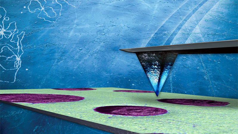
Scanning Tunneling Microscopy (STM)
Atomic resolution on conductive samples
The development of Scanning Tunneling Microscopy (STM) at IBM in the 1980s won Gerd Binnig and Heinrich Rohrer the 1986 Nobel Prize in Physics. This technique served as the groundwork for the subsequent advancement to Atomic Force Microscopy (AFM). STM measures topography of surface electronic states using a tunneling current that is dependent on the separation between the probe tip and a sample surface.
STM is typically performed on conductive and semiconductive surfaces. Common applications consist of atomic resolution imaging, Scanning Electrochemical Potential Microscopy (SECPM), and low current imaging of less conductive samples.
In-situ atomic resolution electrochemical STM image of Cu underpotential deposition on Au(111).


