AFM 模式

扫描隧道显微镜 (STM)

导电样品可达原子分辨率

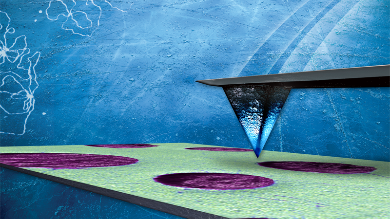
IBM 于 1980 年代开发了扫描隧道显微镜(STM),发明人Gerd Binnig 和 Heinrich Rohrer 因该成果荣获 1986 年诺贝尔物理学奖。该技术为后来进一步发展到原子力显微镜(AFM)奠定了基础。STM 采用隧穿电流来测量表面电子状态的形貌,其隧穿电流取决于探针针尖与样品表面之间的距离。

STM 通常用于导体和半导体表面测量。常见应用包括原子分辨率成像、扫描电化学电位显微镜(SECPM)以及对导电性不良的样品进行低电流成像。

铜在金(111)表面的欠电位沉积的原位原子分辨率电化学 STM 图像
Input value is invalid.

Get instant access to the full-length AFM modes handbook.

The Definitive AFM Modes Handbook contains everything you need to understand, select, and apply AFM techniques in materials research, including:

  • An easy-to-use framework for understanding the seven categories of AFM modes, their capabilities, and their core uses
  • Detailed descriptions of 50+ modes and variants (including 300+ data images)
  • Summary information about what each mode is, how it works, and when to use it
  • Our experts' top probe recommendations for each mode
Please enter your first name
Please enter your last name
Please enter your e-mail address
Please enter a valid phone number
Please enter your Company/Institution
What best describes your current interest?
Please accept the Terms and Conditions

             Privacy Notice   Terms of Use


  * Please fill out the required fields.

Your download is now available.


Note:
If you exit this page, you may not be able to reopen this download window without re-submitting the form.