
QCVelox-HR
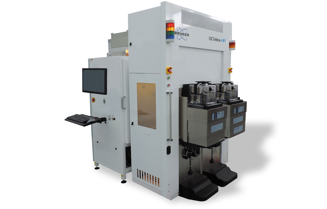
QCVelox-HR
QCVelox-HR is the highest productivity high-resolution X-ray diffraction (HRXRD) and X-ray reflectivity (XRR) metrology system for complex epilayer structures. HRXRD measures the crystal quality, strain, relaxation, and thickness of the epilayers, while XRR determines their thickness, density, and surface roughness. QCVelox-HR features full automation and factory integration software for production line metrology. Once data is collected, Bruker’s powerful analysis software accurately and reliably gives epilayer process parameters, with automatic reporting and immediate feedback to control and monitor production lines.
Fully Automated Operation for Improved Process Control

QCVelox-HR provides fully automated epilayer quality control. It delivers detailed information on properties, including composition, thickness, and uniformity. This full characterization of critical structure parameters ensures that epitaxial layers and films meet specifications necessary for high-performance devices.
Only QCVelox-HR delivers:
- Industry-leading high-throughput X-ray metrology for compound semiconductor manufacturing.
- Enhanced device performance and yield through fully automated epilayer quality control.
- Reliable measurements and results reporting with a suite of powerful and dependable software.
Automated sample loading, alignment, and measurement with QCVelox-HR produces reliable metrology data, which is then automatically analyzed and reported using Bruker’s industry-leading data analysis software. The tool’s fully automated, high-precision epilayer quality control enables manufacturers to:
- Shorten the R&D cycle
- Develop high-performance devices
- Reduce time to market
- Accelerate production ramp
- Fully optimize yield through control of key parameters
- Improve quality and reliability during mass production

Highest Throughput
High throughput and precision enable higher sampling rates per wafer, allowing manufacturers to identify process issues early, improving product quality and reducing waste. Bruker has incorporated numerous unique design features to achieve the fastest possible measurements with high precision. This innovation is backed by our extensive experience and expertise in providing cutting-edge, reliable equipment to the semiconductor industry.
Seamless Integration
Leveraging extensive inline experience in fully automated fabs, Bruker has developed industry-leading software for automated analysis and reporting. Essential features are integrated, including batch fitting functionality for offline data analysis, automated wafer reports with pass/fail criteria, and optional reporting via SECS/GEM.
QCVelox-HR Automation and Facilities Specifications
Each wafer manufacturing facility and semiconductor fab has its own specific requirements and challenges. Our listed product specifications and offerings are always a starting point for a conversation with our experts to determine how our capabilities can meet your needs.
| Wafer Handling | Wafer robot with open cassette up to 200 mm; EFEM 200 mm-300 mm FOUP, 150 mm-200 mm SMIF |
| SECS/GEM | Yes |
| Cleanliness Specification | ISO Class 3 |
| Standards Compliance | SEMI S2, S8, S14, S22, S23, F47 |
| Footprint (with EFEM) | 1.35 m x 2.6 m |