FilmTek 4000

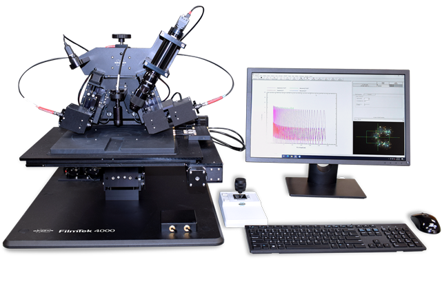
FilmTek 4000
The FilmTek™ 4000 is optimized for high resolution measurement of refractive index required for silicon photonics and waveguide applications. Utilizing multi-angle reflectometry and patented multi-angle Differential Power Spectral Density analysis capability, the FilmTek 4000 delivers unmatched measurement accuracy for refractive index. Measurement resolution is optimized through independent thickness and index (TE and TM modes) measurements, with index measurement resolution up to 2×10⁻⁵. This provides a 100x performance advantage over the best non-contact method and 10x that of the best prism coupler contact systems. When equipped with optional spectroscopic ellipsometry, the tool can also measure very thin films.
Measurement Capabilities
Enables simultaneous determination of:
- Multiple layer thicknesses from 0Å to 250µm (with SE option)
- Optical properties from 400nm-1700nm
- TE and TM indices of refraction [ n(λ) ]
- Extinction (absorption) coefficients [ k(λ) ]
- Energy band gap [ Eg ]
- Constituent, void fraction
System Components
Standard:
- Multi-angle, polarized spectroscopic reflection (400nm-1700nm)
- Patented Multi-Angle Differential Power Spectral Density (MADP) analysis
- Patented Differential Power Spectral Density (DPSD) processing
- Measures film thickness and index of refraction independently
- 2×10⁻⁵ refractive index resolution
- Whole wafer measurement
- Automated stage with autofocus
- Automated beam alignment
- Camera for imaging measurement location
- Advanced material modeling software
- Bruker's generalized material model with advanced global optimization algorithms
Optional:
- Spectroscopic ellipsometry with rotating compensator design
- Hot plate for characterization of refractive index and thermal expansion as a function of temperature
- Cassette to cassette wafer handling
- FOUP and SMIF compatible
- Pattern recognition (Cognex)
- SECS/GEM
FilmTek 4000 Methodology
FilmTek 4000 systems employ our patented DPSD (Differential Power Spectral Density) technique for high precision refractive index measurement. Spectroscopic reflection data are gathered at normal incidence and 70 degrees. PSD processing results in two peaks in the Power Spectral Density domain. The ratio of their positions is a function of the index of refraction of the film, and the angle of incidence of the oblique measurement. This ratio is used to calculate the index. Once the index is known, the thickness can be calculated from the optical thickness of the normal incident peak.
Typical Application Areas

Silicon Photonics
Measure film thickness and refractive index with a 10x performance advantage over the best prism coupler contact systems.
Filmtek non-contact multi-angle reflectometry systems deliver precise high-resolution measurements and enable automated, in-line process control for a wide range of planar waveguide and silicon photonics applications (e.g., SiON, Si3N4, Ge-SiO2, P-SiO2, BPSG, APOX, HiPOX, and multi-layer SiO2/ SiON film stacks).
Technical Specifications
| Film Thickness Range | 0 Å to 250 µm (with SE option) |
|---|---|
| Film Thickness Accuracy | ±1.5 Å for NIST traceable standard oxide 5000 Å to 1 µm |
| Precision (1σ) | 5 µm Oxide (t,n): 2Å / 0.00002 |
| Spectral Range | 380 nm - 1700 nm (380 nm - 1000 nm is standard) |
| Measurement Spot Size | 1 mm (normal incidence); 2 mm (70°) |
| Sample Size | 2 mm - 300 mm (150 mm is standard) |
| Spectral Resolution | Visible: 0.3 nm / NIR: 2 nm |
| Light Source | Regulated halogen lamp (10,000 hrs lifetime) |
| Detector Type | 2048 pixel Sony linear CCD array / 512 pixel cooled Hamamatsu InGaAs CCD array (NIR) |
| Automated Stage | 150 mm - 300 mm (200 mm is standard) |
| Computer | Multi-core processor with Windows™ 10 Operating System |
| Measurement Time | <5 sec per site (e.g., oxide film) |
How Can We Help?

Bruker partners with our customers to solve real-world application issues. We develop next-generation technologies and help customers select the right system and accessories. This partnership continues through training and extended service, long after the tools are sold.
Our highly trained team of support engineers, application scientists and subject-matter experts are wholly dedicated to maximizing your productivity with system service and upgrades, as well as application support and training.