Dimension IconIR
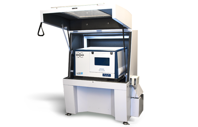

Dimension IconIR
布鲁克大样品台Dimension IconIR系统将纳米红外光谱技术(AFM-IR)和扫描探针技术(SPM)集成到一个平台,为学术界和工业界用户提供先进的纳米光谱、化学成像和物理性质成像工具。IconIR结合了数十年的研究和技术创新,基于Dimension Icon ®原子力显微镜的最新平台,实现卓越的纳米级属性成像能力。该系统支持相关的显微镜和化学成像,具有超高空间分辨率和单层灵敏度,同时其独特的大样品台结构,提供极大的样本灵活性,大大扩展应用领域。
凭借先进的红外激光光源,精心的系统设计和用户友好的操作模式,布鲁克Dimension IconIR平台为用户提供优异的纳米光谱检测。详情请参考应用指南“Dimension IconIR-高性能纳米尺度红外光谱和成像系统”。
To learn more, continue reading, contact us, or see FAQs about this product.
卓越的纳米红外功能和性能

在单个系统中,IconIR提供高性能纳米级红外光谱、化学成像分辨率和单分子层灵敏度。
Dimension IconIR提供:
· 与FTIR高度一致的高性能纳米红外光谱,优于10nm化学成像分辨率和单分子层灵敏度
· 化学成像可与PeakForce Tapping®纳米机械和纳米电学关联
· 高性能AFM成像和极大的样品灵活性,可容纳大尺寸样品*
· 广泛适用的应用组件和AFM功能模块
*标准系统支持150mm大样品,也可提供能够容纳更大样品的版本
完整的关联研究显微镜
集成Bruker特有的PeakForce轻敲纳米物性成像和纳米红外光谱技术,Dimension IconIR系统的大样本平台特别适合于电学或化学反应环境中材料和活性纳米系统,甚至是具有强机械异质性的复杂系统的关联研究。
IconIR提供:
先进的定量属性成像技术
用于定量纳米化学,纳米机械和纳米电学表征的完整关联研究方案


高性能纳米红外光谱

布鲁克是基于光热AFM-IR纳米红外光谱技术的发明者,并拥有多项专利和独特的纳米红外模式。这些模式使IconIR能够提供与FT-IR光谱一致的高速、高性能光谱。模式的多样性为工业和学术用户的广泛样本提供测试支持。
IconIR提供:
与FT-IR一致的高性能,丰富,详细的光谱,实现单分子光谱
共振增强AFM-IR,纳米红外领域的首选技术,已发表大量科学出版物
高性能轻敲模式AFM-IR光谱
超高分辨率化学成像
Icon业界领先的AFM性能和Bruker专利的轻敲AFM-IR成像共同提高了纳米红外技术的空间分辨率和样品适用性,并将其应用扩展到光热AFM-IR技术目前尚未解决的领域。
IconIR提供:
· 优于10nm的空间分辨率,用于广泛的材料类型(包括软质材料)的化学成像
· 分子层灵敏度用于薄膜及生物结构成像
· 一致,可靠,高质量的可发表数据
· 聚合物薄膜的可靠表面敏感化学测量

浅表面化学信息检测

采用布鲁克最新专利表面灵敏模式,IconIR将探测深度从500纳米降低到数十纳米,无需制备截面,无缝结合高空间分辨率和高表面灵敏度。
Dimension IconIR for Nanoscale Chemical and Surface Analysis
The Dimension IconIR enables correlative nanoscale chemical, mechanical, electrical, and morphological characterization by combining nanoIR spectroscopy with PeakForce Tapping–based AFM property mapping on a large‑sample platform. It is designed for studies that require high‑resolution chemical imaging with direct FT‑IR correlation, alongside nanomechanical and nanoelectrical measurements on the same sample area.Representative applications include:
- Nanoscale chemical imaging/spectroscopy with sub‑10 nm spatial resolution, monolayer sensitivity
- Correlative nanochemical, nanomechanical, and nanoelectrical mapping using nanoIR spectroscopy combined with PeakForce Tapping modes
- Polymer blends and block copolymers, including PS‑LDPE blends and PS‑b‑PMMA systems, with clear chemical contrast between phases
- Thin films and layered materials, where monolayer‑level chemical sensitivity is required
- Composite and embedded materials, such as carbon fibers in epoxy, requiring correlated chemical and property mapping
- Large or non‑standard samples, enabled by the system’s large‑sample architecture and motorized positioning stage
- Materials research in electrically or chemically active environments, using a broad range of AFM modes and accessories
LEARN MORE:
Polystyrene & Polyethylene Blend
In this first real‑time demonstration, a Bruker nanoIR applications expert investigates a polystyrene and low‑density polyethylene (LDPE) blend in which LDPE forms globules on the surface of a polystyrene matrix.
- Using Bruker NanoScope® software, the session starts with topography, then introduces PLL1 frequency, tapping phase, and IR channels to build material contrast. By targeting aromatic bands in polystyrene and the polyethylene backbone, the demo shows strong chemical contrast between the two materials, including contrast inversion when the laser wavenumber is changed.
- Uses PLL1 frequency data to confirm a clean IR response independent of spectral artifacts, demonstrating true chemical sensitivity. The video concludes with spectroscopy measurements, including line scans and point spectra, clearly differentiating polystyrene and LDPE based on their infrared signatures.
This second demonstration revisits the same polystyrene and low‑density polyethylene (LDPE) blend using PeakForce KPFM to correlate chemical, mechanical, and electrical properties within a single measurement workflow.
- Collects electrical property data simultaneously, revealing how local electrostatics and polymer chemistry influence the measured work function.
- Demonstrates co‑localized chemical, mechanical, and electrical mapping, with the same LDPE and polystyrene features visible across all channels.
- Highlights the advantage of true co‑local measurement, eliminating the need to infer relationships between chemistry, mechanics, and electrical behavior from separate experiments.
- Provides a complete, spatially consistent picture linking composition directly to material behavior at the nanoscale.
In this third real‑time demonstration, a Bruker nanoIR applications expert shows nanoscale chemical and mechanical characterization of a polystyrene and low‑density polyethylene (LDPE) blend, highlighting simultaneous multi‑channel measurement capabilities.
- Collects AFM topography, modulus, adhesion, and IR signal in a single pass, revealing LDPE features in polystyrene matrix.
- Demonstrates UI‑guided point selection for nanoscale IR spectroscopy, with ~5 s per point acquisition.
- Correlates AFM‑IR data with FTIR spectra for material identification.
- Uses offline analysis to clearly differentiate IR signal and spectral features of LDPE versus polystyrene domains.
PS-PMMA Blend
In this real‑time demonstration, Dimension IconIR is used for correlative chemical, mechanical, and morphological analysis of a 1:1 polystyrene/PMMA polymer blend.
- Begins with AFM topography and phase imaging, showing limited material contrast and an apparent (misleading) homogeneity.
- Uses AFM‑IR to reveal heterogeneity; nanospheres and clear phase segregation between PMMA and polystyrene domains.
- Demonstrates simultaneous AFM and IR data collection, enabling direct correlation of morphology, mechanics, and chemistry.
- Confirms blend composition and visualizes component distribution through phase‑resolved chemical mapping.
PMMA Beads in Epoxy
This first demonstration uses tapping AFM‑IR to identify and differentiate chemical species in a sample containing PMMA beads embedded in an epoxy matrix on a thick sulfite substrate.
- Overlays the AFM image with the optical image, precisely locating measurement area.
- Performs four point spectroscopy measurements (two on the matrix, two on PMMA particles), with three repeat sweeps per point (10 s each).
- Shows clear, repeatable spectral differences between matrix and particles, including a distinct carbonyl band, with intensity variations linked to local thickness.
- Acquires AFM‑IR images at 1510 and 1730 wavenumbers, producing contrast inversion between PMMA and epoxy.
- Confirms chemical contrast and material identity through correlation with FTIR spectra.
This second demonstration showcases selective, high‑acuity nanoscale chemical and mechanical analysis on a microtomed epoxy film containing embedded PMMA beads, polystyrene beads, and carbon black.
- Demonstrates highly targeted AFM‑IR measurements, selecting specific PMMA beads and tuning the IR wavelength to probe the carbonyl band in PMMA and chemical features of the epoxy resin.
- Switches between sample- and tip-scanning modes, illustrating workflow flexibility and access to legacy Bruker modes.
- Uses PeakForce QNM in air on the same sample to collect mechanical data.
- Shows that, despite similar elastic moduli, PMMA, polystyrene, and epoxy can be mechanically distinguished, enabling material discrimination independent of tapping mode typically used for AFM‑IR.
- Demonstrates how chemical and mechanical properties can be decoupled and analyzed in a single, correlative workflow.


Frequently Asked Questions
Dimension IconIR supports Tapping AFM-IR and Resonance Enhanced AFM-IR as standard modes. Surface Sensitive AFM-IR and REFV AFM-IR are available as options, depending on the system’s configuration and accessories.
IconIR supports samples up to 150 millimeters in diameter and is designed for either multiple coupons or large-sample workflows. Bruker also has the Dimension IconIR 300 for full access on 200 mm and 300 mm wafers. If you need to work with larger or heavier samples, consult Bruker for custom solutions.
Standard Dimension Icon AFMs cannot be routinely upgraded to IconIR systems. IconIR is a dedicated platform with integrated IR capability.