FilmTek 2000M TSV Robotic
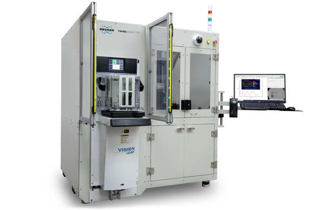
FilmTek 2000M TSV
The FilmTek™ 2000M TSV is a fully automated metrology tool that utilizes non-destructive optical technology to measure film thickness, through-silicon via (TSV) depth, trench depth, CD, and total thickness variation (TTV) in both front-end and advanced packaging development applications. 2000M TSV’s patented optical design generates a highly collimated beam with small spot size, uniquely enabling thickness measurements of thick films up to 350 µm, depth measurements of HAR TSV structures with diameters down to 2 µm and aspect ratios of 40:1, and evaluation of the smallest test pads with its variable spot size down to 2x1 µm. 2000M TSV is a versatile, high-performance tool ideal for high-volume semiconductor manufacturing or research and development facilities.
2000M TSV's unmatched versatility and performance make this system uniquely well-suited for high-volume semiconductor manufacturing, MEMS foundries, R&D, and shared common development facilities.
Film Thickness Measurements
Unlike typical reflectometry tools, FilmTek 2000 TSV uses collimated light. A collimated beam makes it possible to maintain coherent reflectance for thin to very thick films, producing accurate thickness measurements from films 5 nm to 150 µm thick in the standard configuration.
Combined with a high-resolution spectrometer, 2000M TSV can fit and model high-frequency oscillations common in thick film reflectance data, extending the compatible film thickness to 350 µm.

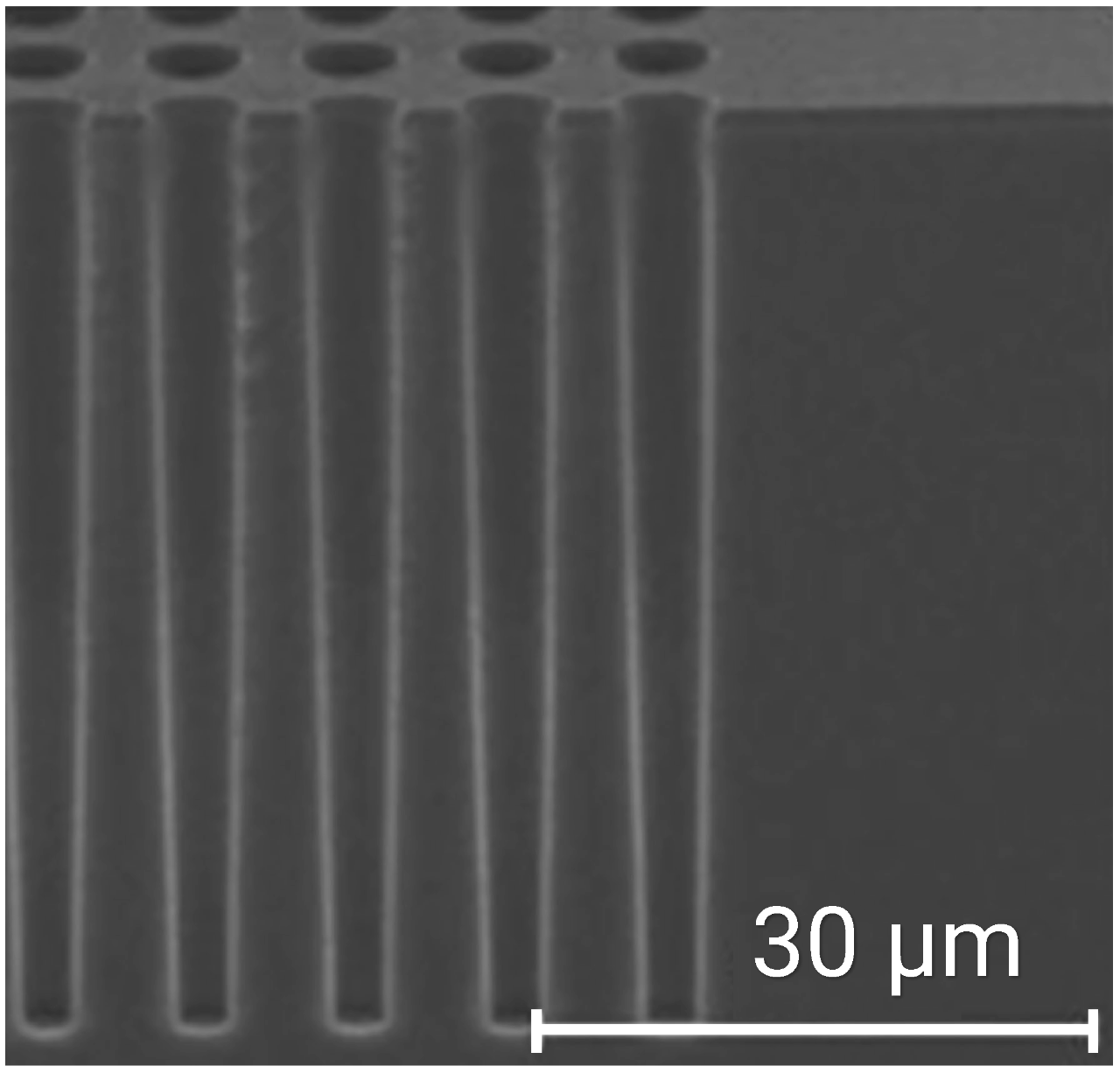
High Aspect Ratio TSV Characterization
Typical reflectometry tools also cannot reliably measure the depth of through-silicon via (TSV) structures due to incoherence. The collimated beam and small spot size of FilmTek 2000M TSV make it able to reach the bottom of high aspect ratio structures like TSV, accurately measuring diameters down to 2 µm and aspect ratios of 40:1.
Patented TSV data processes allow for a simple reflectance measurement to give detailed real-time results for TSV depth and CD analysis. The integrated CCD camera is used to measure top CD and for other imaging purposes.
Next-Gen Semiconductor Process Control
As the semiconductor industry moves towards increasingly smaller devices, metrology tools must keep pace. 2000M TSV’s patented optical design has a variable spot size that can go as small as 2x1 µm, capable of measuring the smallest test pads in extremely tight spaces.
From front-end manufacturing to advanced packaging and hard drive applications, FilmTek 2000M TSV can measure thin and thick layers on top of and around devices to provide process control and reduce scrap.
Typical Application Areas

Semiconductor Manufacturing
Perform fast, accurate, and repeatable multi-layer film thickness and refractive index measurements on patterned device wafers for semiconductor manufacturing.
FilmTek systems enable process control of oxides, nitrides, ONO, Oxide / Nitride / Cu, polysilicon / oxide, AlN, TaN, TiN, SiGex and composition control, resist, Si3N4/GaAs, ARC, gate oxide, and GaAs films, CMP on Cu, and many other materials encountered throughout the entire wafer fabrication process.

Advanced Packaging
Measure the complete range of back-end manufacturing and process control packaging parameters.
FilmTek process control solutions enable fully automated measurements for thick resist thickness for bump coplanarity, high-aspect-ratio TSV depth and top CD for interconnects, bonded silicon thickness or Total Thickness Variation (TTV), and thin metal-oxide thickness in bonding processes to prevent non-wet open failures.
Typical application areas include:
- TSV metrology
- Advanced semiconductor packaging

MEMS
Perform fully-automated film thickness and refractive index measurements of oxide, nitride, oxide/nitride, ONO, amorphous carbon, resist, and oxide/polysilicon/oxide films on patterned device wafers.
Fully-automated FilmTek ellipsometry and reflectometry tools feature cassette-to-cassette wafer handling, 50µm spot size, pattern recognition, and SECS/GEM with a best-in-class combination of performance and price.
TSV Depth Variation
Getting an overall view of thickness or TSV depth variations across an entire wafer can be vital to effective process control. Here, a 26-point patch plot shows TSV depth variation across a 300 mm wafer.

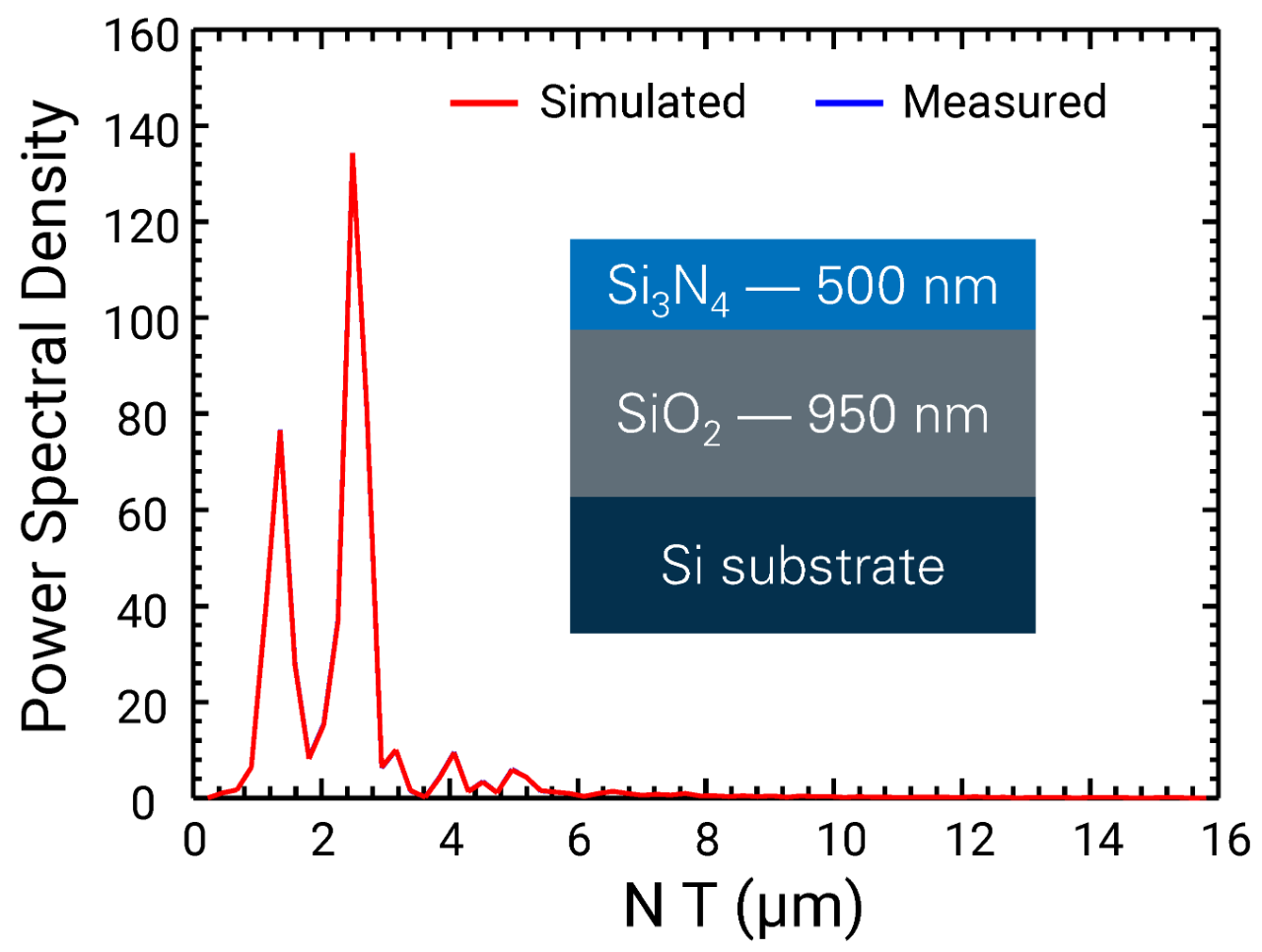
Depth Measurement Accuracy for TSVs
Via etch depth measurements were measured with the 2000M TSV and compared against destructive SEM cross-sectional measurements. Results showed close agreement between the two measurements for via diameters 5–20 µm.

FilmTek 2000M TSV Select Specifications
Each wafer manufacturing facility and semiconductor fab has its own specific requirements and challenges. Our listed product specifications and offerings are always a starting point for a conversation with our experts to determine how our capabilities can meet your needs.
| Measurement Function | TSV etch depth, bump height, critical dimension, and film thickness |
| Substrate Size | 200 or 300 mm |
| CD Precision (1σ) | <0.2% |
| Etch Depth Precision (1σ) | <0.005% |
| Film Thickness Range | 5 nm to 350 µm (5 nm to 150 µm is standard) |
| Film Thickness Precision (1σ) | <0.005% |