Application Note: Performing High Strain Rate Testing at Elevated Temperature with SEM PicoIndenters
In-Situ Nanoindentation at High Strain Rates with PI 89 and PI Envision
High strain rate loading is common in real‑world events, such as vehicle crashes, drop and impact loading, ballistic penetration, and high‑speed machining. Under these conditions, materials often exhibit higher apparent strength, reduced ductility, and distinct failure modes compared to slow loading conditions. In‑situ scanning electron microscope (SEM) nanoindentation testing at high strain rates provides insight that quasi‑static measurements and post‑test analyses cannot; it resolves the onset of plasticity, shows how strain localizes, and visualizes the process of crack nucleation and growth.
In this application note, we introduce in‑situ high strain rate indentation in the SEM and present a case study quantifying the strain‑rate sensitivity of tungsten at a high temperature.
Readers can expect to find:
- An overview of high strain rate testing and its real-world applications
- Advantages of using in-situ SEM nanoindentation for high strain rate testing
- A case study illustrating the determination of strain-rate sensitivity for tungsten at 250°C
KEYWORDS: Nanoindentation; Hysitron; Application Note; Bruker; AN1552; PI 89; PI Envision; SEM PicoIndenter

Importance of In‑Situ High‑Strain‑Rate Testing
Rapid loading occurs in instances such as vehicle crashes, explosions, ballistic events, and sudden mechanical shocks. During such events, inertia effects become significant and deformation can localize, often leading to phenomena such as adiabatic shear band formation or brittle fracture. Applications requiring high strain rate testing span a wide range of fields:
- Automotive and aerospace—designing structures that can withstand extreme loading rates, improving crashworthiness, and developing lightweight impact resistant materials.
- Defense—evaluating armor performance and penetration resistance.
- Microelectronics, and MEMS—understanding rapid loading for drop impacts or thermal shocks.
- Nuclear materials research—assessing behavior of irradiated material during accident scenarios.
In‑situ high strain rate testing is particularly valuable because it allows direct observation material deformation and failure during rapid loading, rather than relying on post-test analysis or indirect measurements. When combined with techniques such as SEM or high‑speed imaging, in‑situ testing enables researchers to observe where plastic deformation initiates, how strain localizes, and how cracks nucleate and propagate in real time. This provides critical insight into deformation mechanisms that cannot be captured through conventional testing.
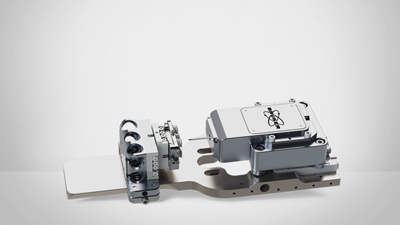
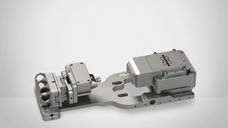
The Hysitron PI 89 and PI Envision SEM PicoIndenters are capable of performing high strain rate mechanical testing using high‑stiffness transducers (500 mN and 3.5 N) equipped with Direct Drive (DD) piezo flexure actuation. PI 89 can achieve maximum strain rates exceeding 1000 s‑1, while PI Envision supports strain rates greater than 100 s‑1, allowing users to probe material behavior across a wide range of dynamic deformation regimes. A key advantage of both systems is that no additional or specialized hardware (beyond what is needed for quasi‑static testing) is required to perform high‑strain‑rate testing. High‑strain‑rate experiments can be conducted not only at room temperature, but also under cryogenic and elevated temperature conditions.
Case Study: Strain‑Rate Sensitivity from Room Temperature to 250°C
Methods
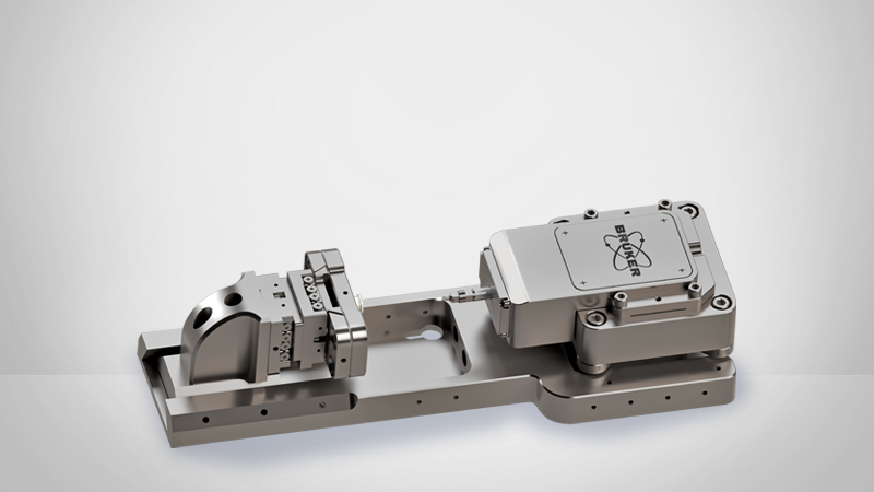
All tests were performed on a Hysitron PI 89 SEM PicoIndenter equipped with a Direct Drive (DD) piezo flexure (maximum displacement of 30 µm) and an xR High Load transducer (maximum force of 3.5 N). Indentations were performed at constant, defined strain rate in displacement control to a maximum depth of 1000 nm. Here, strain rate is defined as ḣ / h which is the ratio of displacement rate to the displacement.2 This loading condition requires displacement to follow an exponential function of time.
PI 89 is capable of maintaining the same strain rates, up to about 1000 s‑1, over a wide temperature range. For this study, fused quartz, a nanoindentation standard specimen, was tested using a diamond Berkovich probe at room temperature with strain rates of 1, 10, 100, and 500 s‑1. Polycrystalline tungsten with ~30 µm grain size was tested using a cubic boron nitride (cBN) Berkovich probe at 250°C with strain rates of 1, 10, 100, and 1000 s‑1. The tungsten sample was ground with SiC metallographic paper down to 1200 grit before polishing with diamond suspension (3 µm, 1 µm) and finishing with 0.03 µm colloidal silica.
Due to the high speeds at which indentation is performed, typical nanoDynamic (oscillatory) testing to continuously measure the contact depth, hc, is not possible. Instead, assumptions must be made to calculate the depth dependence of mechanical properties at high speeds. One common assumption is that the ratio of contact depth to total displacement is constant throughout the indentation, i.e., hc / h ="constant".2 This, along with the calibrated area function from the standard Oliver–Pharr approach1 , allows calculation of hardness throughout the test. Strain‑rate sensitivity, m = ∂lnH / ∂lnε̇, describes the change in yield strength (or hardness) as the applied strain rate changes.3

Results
Figure 1a shows the strain rate and hardness profiles at room temperature on fused quartz. As expected, the hardness varies little between strain rates because the deformation of fused quartz is strain‑rate insensitive. Figure 1b shows the strain rate and hardness profiles on the tungsten specimen indented at 250°C. Here, there is substantial variation in the measured hardness as the strain rate is increased.
Hardness versus strain rate can be plotted on a log‑log plot, as seen in Figure 2, to calculate the strain‑rate sensitivity of the material. The slope of the fit in Figure 2 is m, the strain‑rate sensitivity, and is approximately equal to 0.05 at 250°C. This change is in good agreement with previous measurements made on single‑crystal tungsten.4

PI 89 and PI Envision Enable In‑Situ High‑Strain‑Rate Indentation in the SEM
Controlled, quantitative in‑situ high strain rate nanoindentation testing in the SEM from room temperature to high temperature can be achieved using Hysitron PI 89 and PI Envision SEM PicoIndenters without specialized add‑ons. In the presented case study, a strain rate–insensitive reference showed stable hardness across the tested range, whereas tungsten at 250°C exhibited clear positive rate dependence with strain‑rate sensitivity of ~0.05. These high‑strain‑rate testing capabilities, especially the ability to perform experiments at elevated temperatures, is valuable for industry sectors where rapid loading occurs, such as automotive, aerospace, defense, microelectronics, and nuclear.
Authors
- Kevin Schmalbach, Ph.D., Staff Scientist (kevin.schmalbach@bruker.com)
- Sanjit Bhowmick, Ph.D., NI Product Line Manager (sanjit.bhowmick@bruker.com)
- Eric Hintsala, Ph.D., Manager NI Applications Development (eric.hintsala@bruker.com)
References
- Oliver, W.C., Pharr, G.M. 1992. "An improved technique for determining hardness and elastic modulus using load and displacement sensing indentation experiments", J. Mater. Res. 7: 1564–1583. DOI: 10.1557/JMR.1992.1564
- Hackett, B.L., Sudharshan Phani, P., Walker, C.C., et al. 2023. "Advances in the measurement of hardness at high strain rates by nanoindentation", J. Mater. Res. 38: 1163–1177. DOI: 10.1557/s43578‑023‑00921‑1
- Maier, V., Schunk, C., Göken, M., and Durst, K. 2015. "Microstructure-dependent deformation behaviour of bcc-metals – indentation size effect and strain rate sensitivity", Philos. Mag. 95: 1766. DOI: 10.1080/14786435.2014.982741
- Kappacher, J., Leitner, A., Kiener, D., et al. 2020. " Thermally activated deformation mechanisms and solid solution softening in W-Re alloys investigated via high temperature nanoindentation", Mater. Des. 189: 108499. DOI: 10.1016/j.matdes.2020.108499
@2026 Bruker Corporation. All rights reserved. Hysitron and PicoIndenter are trademarks of Bruker Corporation. All other trademarks are the property of their respective companies. AN1552, Rev. A0.