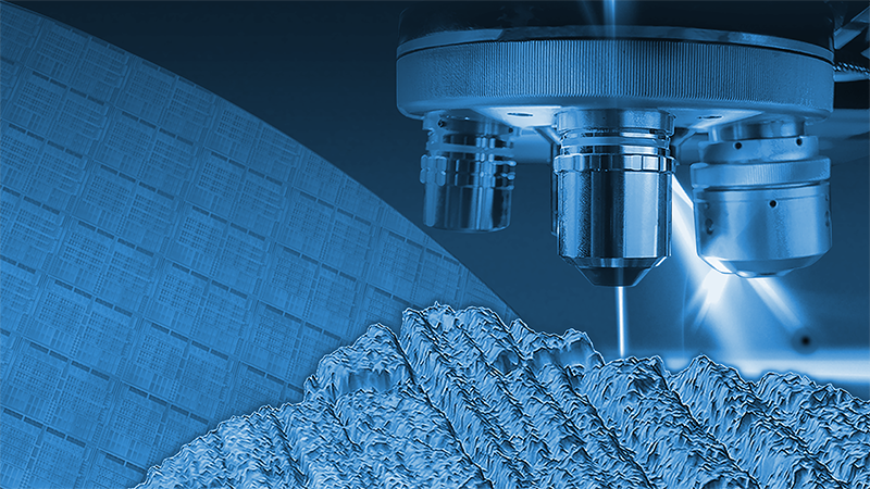
Optical Profiler Characterization of Advanced Materials Using White Light Interferometry
WLI-based characterization techniques are driving innovation in materials research and development.
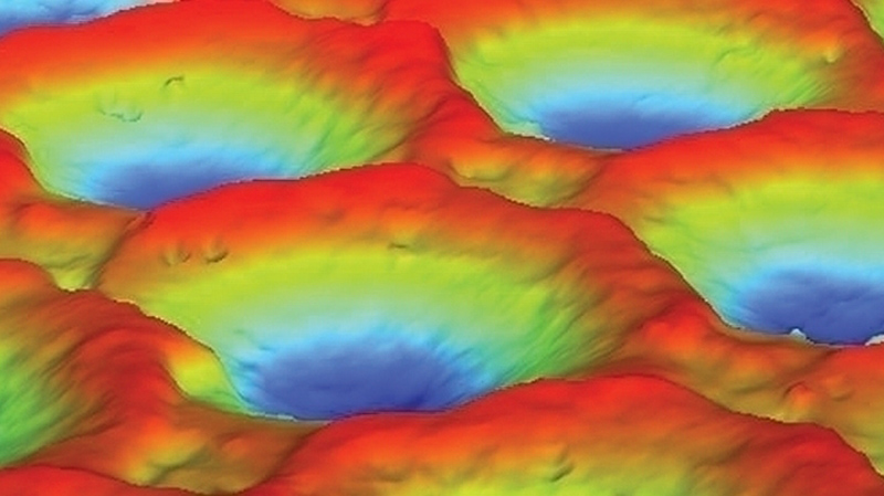
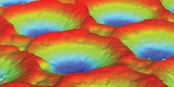
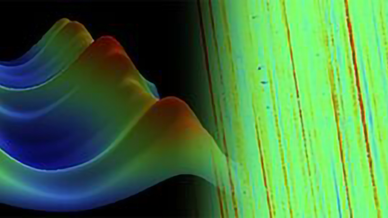
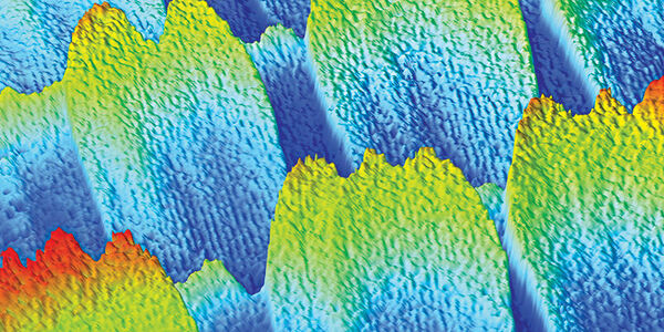
This webinar provides a comprehensive exploration of white light interferometry (WLI)-based advanced materials characterization, including techniques, practical considerations, and regulatory standards for such concepts as waviness, roughness, and spatial filtering.
Webinar Summary
Explore Fast, Accurate Techniques for Advanced Materials Characterization
Tackling global challenges often requires the development of new, increasingly advanced materials; these support efforts to build a neutral carbon dioxide economy, improve energy efficiency, develop high bandwidth communication, and identify better methods for preventing and fighting pandemics, among others.
Yet new materials development evolves quickly, driven by innovation in the capabilities and capacity of R&D equipment and processes. As a result, dedicated, high-performance characterization tools are increasingly important in a wide range of fields ranging from geology to optoelectronics.
Geared toward materials scientists, bio-mechanical researchers, geology & nuclear waste researchers, materials development researchers & engineers, and waveguide optical developers, this webinar includes:
- A comprehensive explanation of roughness considerations like waviness, roughness and spatial filtering;
- Steps for the ISO-compliant set up and post-processing analyses of mean roughness measurements;
- An exploration of both profile and areal based measurements, with emphasis on their differences; and
- Practical examples from experts in the field.
Understand the advanced materials characterization techniques driving innovation in materials research and development
Watch this webinar to gain new insight into:
- When and why to use profile- and areal-based profilometry techniques for advanced materials R&D
- How to set up ISO-compliant measurements and post-processing analyses
- Best practices and key considerations for advanced material research
This webinar was presented on September 22, 2020.
Find out more about the technology featured in this webinar or our other solutions for advanced materials characterization.
Featured Products and Technology
Speakers

Samuel Lesko, Ph.D.
Dir. of Technology and Apps Development for Tribology, Stylus & Optical Profilers, Bruker
Samuel Lesko has over 20 years of optical and stylus profiler applications experience, particularly in using white-light interferometry in a wide variety of fields, from MEMS and semiconductor to automotive and aerospace. He is a member of SME and part of ISO/TC 213/WG committee (areal roughness) and obtained his physics Ph.D. and material science engineering degree at the University of Burgundy in France.

Dr. Alexander Nesterov-Mueller
KIT, Institute of Microstructure Technology, Germany

Dr. Andreas Luttge
MARUM, University of Bremen, Germany