
M&M - Microscopy & Microanalysis
Enhance Your Microscopy Research with Bruker
Discover Bruker’s powerful portfolio of microscopy and spectroscopy solutions and connect with our experts to learn how our technologies are advancing research in materials science, semiconductors, polymers, and life sciences.
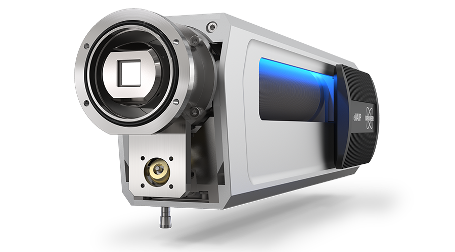
- Be one of the first to see eWARP, the fastest and most sensitive EBSD detector ever, in action. Find out firsthand how this revolutionary detector is changing the microanalysis landscape, facilitating EBSD like never before.
- Learn how the new Dimension Nexus benchtop AFM integrates milestone Bruker innovations into a cost-effective system to deliver wider access to top AFM performance.
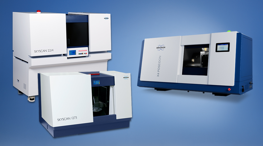
- Discover our portfolio of 3D X-Ray Microscopy (XRM) solutions based on micro-CT technology, featuring the new X4 POSEIDON benchtop 3D-XRM system.
- Discover our range of solutions to enhance electron microscopy with the power to perform elemental and microstructural analysis using techniques such as EDS, WDS and micro-XRF on SEM.
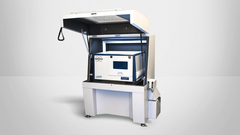
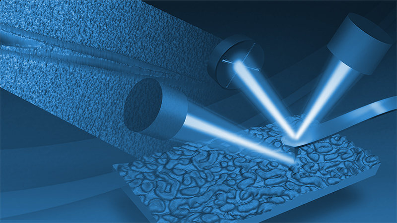
- Explore the power of nanoIR spectroscopy, including the new REFV AFM-IR mode for extended sample compatibility and measurement capabilities.
- See how our Scanning Transmission Electron Microscope, Nion, enables electron microscopy at the atomic scale.
- Experience the advanced capabilities of our PicoIndenters for in-situ nanomechanical testing and precise, high-throughput materials characterization.
If you are interested in learning more about these technologies and how they can enhance your research then visit us at Booth 614 or book a meeting with us at M&M.
Live Demos at the Bruker Booth
DEMO: Enter The New Era of EBSD with eWARP
Register here for a live, one-on-one eWARP demo at the Bruker Booth, number 614, and enter the new era of EBSD.
If you are not able to attend the conference we will also offer live, online demos once the conference has ended. Just select the "online" option in the form.
In addition to eWARP demos we will also be hosting Lunch & Learns, Vendor Tutorials and more - you can find our full program on our M&M event page.

Nion: Scanning Transmission Electron Microscopy at Atomic Resolution
No registration is required for demos on our Nion STEM for atomic scale imaging. Just turn up at the Bruker Booth, number 614, at 4:00pm on Tuesday.
New developments in Cryogenic STEM at liquid Helium temperatures
Tuesday, August 4
New classes of quantum materials of recent interest often require cooling to below LN2 temperatures. Additionally, it is imperative when imaging single crystal specimens in STEM to use a double-tilt specimen holder to enable scanning along intended crystallographic planes. It is a significant challenge to enable both of these instrumentational capabilities simultaneously with a single specimen holder. Here we demonstrate our cryo double-tilt specimen holder to image crystalline materials down to 15 K.
Lunch & Learns at M&M 2026
We’re hosting Lunch & Learns right in our booth, where Bruker scientists present key applications and technologies whilst you enjoy a complementary lunch. Space is limited so make sure to reserve your seat!
Each Lunch & Learn takes place at the Bruker Booth, number 614, at 12:00 PM.
- Monday, August 3:
Maximizing XRM (Micro-CT) Detail with Variable Geometry on the Bruker X4 POSEIDON. - Tuesday, August 4:
eWARP - Best Spatial Resolution, Maximum Throughput, Zero Compromise. - Wednesday, August 5:
Speed Meets Cold: Pushing Nanoindentation Mapping to Cryogenic Temperatures. - Thursday, August 6:
Introduction to STEM.
Vendor Tutorials
Bruker will also be offering Vendor Tutorials after hours in the booth—no RSVP required. Just stop by our booth, grab a seat, and enjoy the insights.
All vendor tutorials will be taking place at the Bruker Booth, number 614, at 5:45 PM.
Monday August 3 - Atomic Force Microscopy - Beyond Imaging: Multimodal Property Mapping with PeakForce Tapping and Fast Force Volume
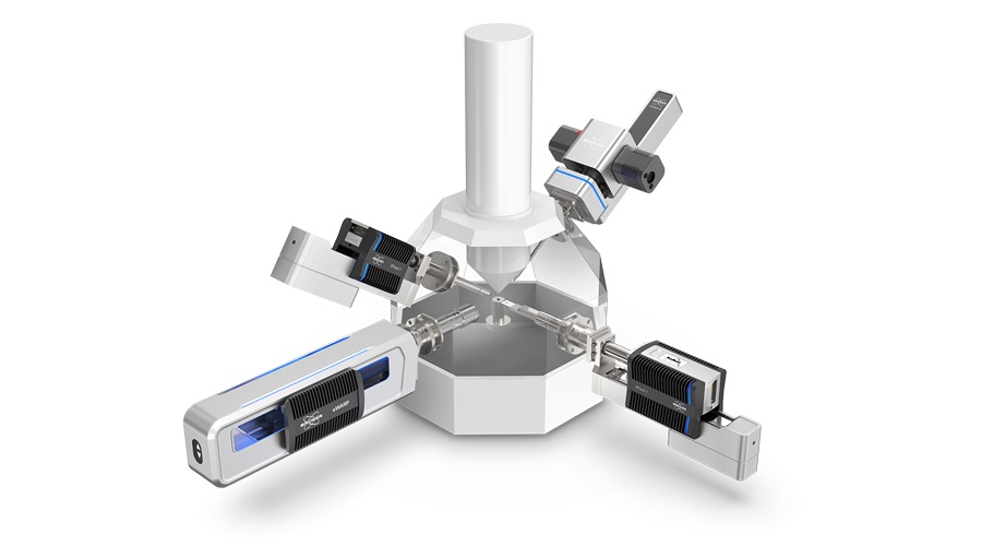
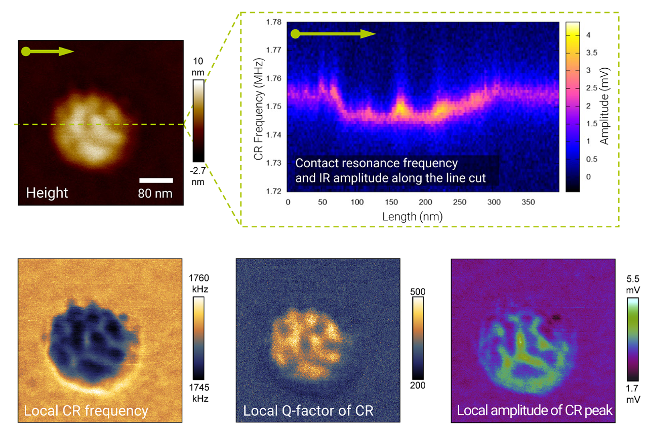
This tutorial reframes PeakForce Tapping (PFT) as a quantitative engine for nanoscale characterization rather than a single imaging mode. We demonstrate how PFT variants—PFTUNA, PFKPFM, PFsMIM, and PeakForce MFM—extend force-controlled interactions into electrical and magnetic domains, while Fast Force Volume (FFV) methods enable high-density, multidimensional datasets including electrical cubes, AFM-nDMA, contact resonance, and REFV-AFM-IR.
Tuesday August 4 - New developments in Cryogenic STEM at liquid Helium temperatures
New classes of quantum materials of recent interest often require cooling to below LN2 temperatures. Additionally, it is imperative when imaging single crystal specimens in STEM to use a double-tilt specimen holder to enable scanning along intended crystallographic planes. It is a significant challenge to enable both of these instrumentational capabilities simultaneously with a single specimen holder. Here we demonstrate our cryo double-tilt specimen holder to image crystalline materials down to 15 K.
Wednesday August 5 - Advanced multi segment EDS detectors with full spectral capability and simultaneous BSE detection
Advanced electron microscopy requires the simultaneous optimization of spatial resolution, analytical sensitivity, and signal throughput. We will present recent developments in multi-segment EDS detector technology, based on Bruker’s XFlash FlatQUAD platform. The detector employs an annular, four-quadrant silicon drift detector (SDD) geometry positioned close to the sample, enabling very high solid angles while maintaining full compatibility with standard SEM operation.
Talks and Poster Presentations at M&M
As part of the symposium program Bruker's experts will be presenting posters at M&M. Make sure to attend to keep up with the latest advances.
Tuesday, August 4
Towards surface science in the STEM: atomic resolution secondary electron imaging on bulk samples
- Session: C08.1 | Speaker: Joel Martis
- Time: 08:45 AM
From Comparative to Coincidence Spectroscopies: Instrumentation for Cathodoluminescence, Light Injection, and EELS in STEM
- Session: A10.2 | Speaker: Luiz Tizei
- Time: 10:45 AM
Stable Liquid-Helium-Cooled STEM with Double-Tilting
- Session: A04.P1 | Speaker: Cameron Johnson
- Time: 03:00 PM
Wednesday, August 5
Unveiling Quantum Order: Cryo-EELS, 4D STEM, and Ptychography at the Nanoscale
- Session: P11.1 | Speaker: Ben Plotkin-Swing
- Time: 09:30 AM
Nano-Optics of Quantum Confined Systems with Electron Spectroscopies
- Session: P8.6 | Speaker: Luiz Tizei
- Time: 10:30 AM
Atomic Resolution Ptychography Movies from 10 Kelvin to Thousands of K, Imaging a Moving Target
- Session: A10.5 | Speaker: Niklas Dellby
- Time: 11:00 AM
Products & Technologies Featured at M&M
eWARP: EBSD Detector with Direct Electron Detection
Enter the new era of EBSD with eWARP - our revolutionary EBSD detector that is changing the microanalysis landscape thanks to its unique direct electron detection technology.
Discover eWARP at M&M by booking a one-on-one demo at the Bruker Booth.
Dimension Nexus Benchtop AFM
Dimension Nexus™ delivers an ideal combination of data quality, experiment flexibility, and ease of use in a small-footprint system. It incorporates the milestone innovations of Bruker's NanoScope® 6 controller, PeakForce Tapping® technology, and ScanAsyst® Plus self-optimizing imaging software to deliver more functionality than competing systems in its class. Suitable for both routine and custom experiments and easily upgradable in the field, Dimension Nexus is both an excellent starter system and a perfect addition to any thriving AFM lab.