

Bruker at TechConnect World Innovation 2025
Visit us at booth 403
June 9–11 | JW Marriott Austin | Austin, TX
Discover our advanced AFM and nanoIR solutions and connect with Bruker experts to learn how our technologies are enabling new frontiers in materials science, polymers, life sciences, and semiconductors.
- Learn how the new Dimension Nexus benchtop AFM integrates milestone Bruker innovations into a cost-effective system to deliver wider access to top AFM performance.
- Explore the power of nanoIR spectroscopy, including the new REFV AFM-IR mode for extended sample compatibility and measurement capabilities.
- See how Bruker’s innovations in AFM and nanoIR systems and operating modes are accelerating research and development across industries.
Conference Host:
Advanced Technology International
Conference Venue:
JW Marriott Austin | Austin, TX
To find out more about this event or the products and technology featured in it:
Bruker Talks
Our scientists will be presenting throughout the conference—stop by to hear case studies, technical insights, and application highlights from Bruker’s thought leaders.
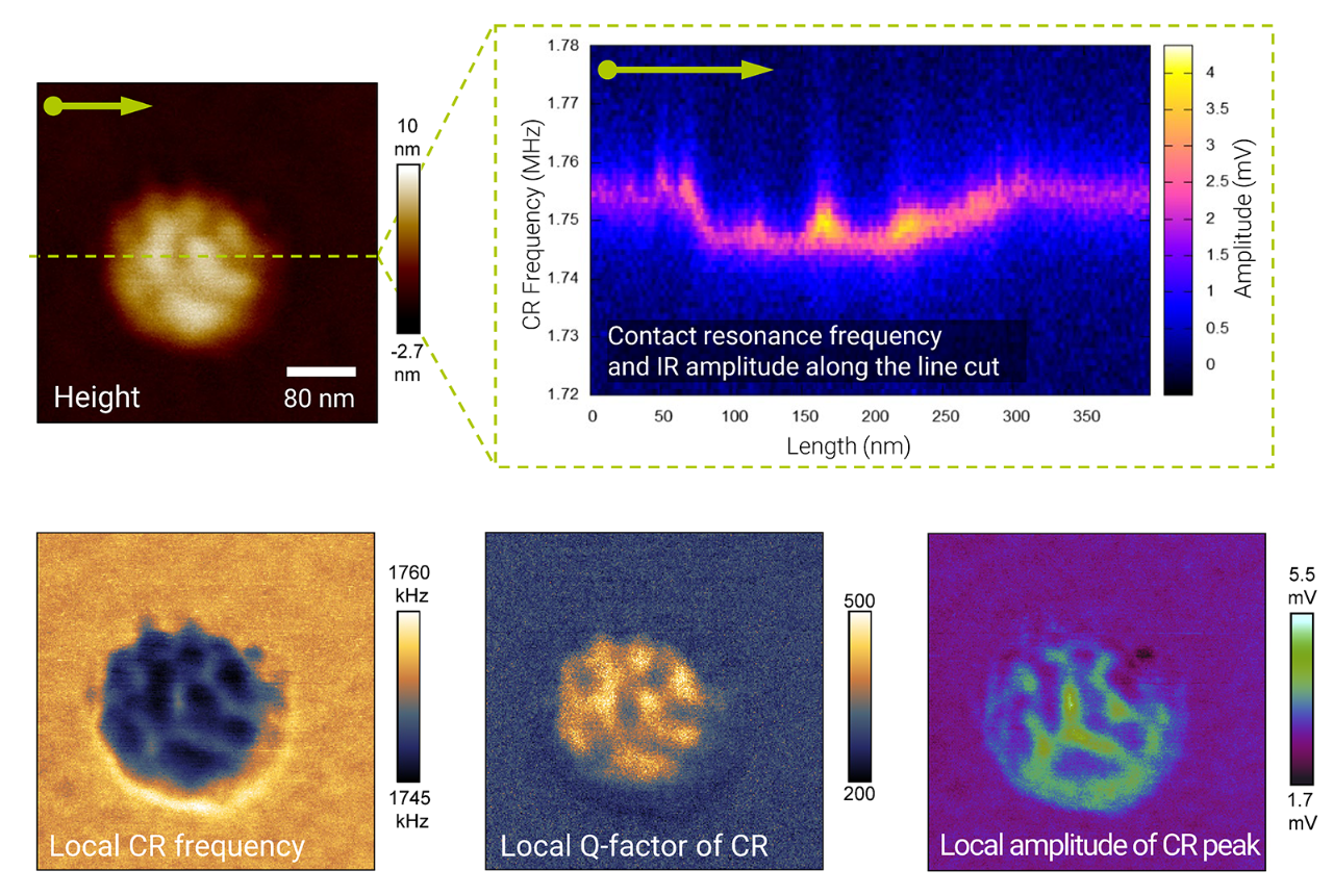
High-resolution mapping of chemical, electrical and mechanical properties via gated sub-resonant intermittent contact AFM
Tapping mode and peak force tapping are intermittent contact AFM modes that provide high-resolution maps of topography and properties by analyzing the bending of a cantilever during oscillation near a sample surface. Since the cantilever is not touching the sample for a significant portion of the oscillation cycle, lateral forces remain small, preventing tip and sample wear. If the oscillation occurs well below the cantilever resonance, the frequency response of the probe is roughly constant and it is possible to directly pick out the details of the tip-sample interaction without deconvoluting the cantilever transfer function. PeakForce QNM uses this method to provide nanoscale maps of mechanical properties such as modulus, dissipation, and adhesion.
The relatively low frequency of oscillation in peak force tapping also facilitates secondary measurements that can then be localized to a point of time (or Z position) in the oscillation cycle as well as a position in the XY plane. For example, current can be measured only while the tip is in contact with the surface or during a fraction of this contact time (typically centered around the point in time where the peak force is reached) [1]. The same "gated" measurement concept has been applied to contact resonance AFM [2], scanning non-linear dielectric microscopy [3], and kelvin probe force microscopy [4] among others. In addition to providing unique new property maps and protecting the tip and sample from damage, these methods benefit from co-located, simultaneous mapping of mechanical properties.
In this talk, we examine the opportunities offered by gated peak force tapping measurements with examples in polymeric materials, semiconductors and 2D heterostructures. The expansion of this approach to other electrical, mechanical & chemical property measurements is reviewed, focusing on properties which are typically collected using contact mode. These operating modes include scanning microwave microscopy (SMIM), scanning capacitance microscopy (SCM), scanning thermal microscopy (SThM), piezoresponse force microscopy (PFM), resonance enhanced AFM-IR, and torsional resonance dynamic friction (TR-DFM also known as torsional force microscopy). We investigate practical aspects of system configuration such as the impact of the position and duration of the ‘gating’ as well as the oscillation frequency on signal-to-noise ratio and signal integrity.
Session Title: SPMConnect: Novel Methods
Date: Tuesday, June 10 th | 3:00 pm
Authors/Presenters: B. Pittenger, C. Li, S. Hu, P. De Wolf
Keywords: AFM, TUNA, sMIM, PFM, PeakForce QNM, peak force tapping
Speaker
Bede Pittenger, Ph.D., Sr. Staff Development Scientist, AFM Applications, Bruker Nano Surfaces
Dr. Bede Pittenger is a Senior Staff Development Scientist in the AFM Unit of Bruker's Nano Surfaces Business. He received his PhD in Physics from the University of Washington (Seattle, WA) in 2000, but has worked with scanning probe microscopes for 25 years, building systems, developing techniques, and studying properties of materials at the nanoscale. His work includes more than thirty publications and three patents on various techniques and applications of scanning probe microscopy. Dr. Pittenger's interests span topics from interfacial melting of ice, to mechanobiology of cells and tissues, to the nanomechanics of polymers and composites.
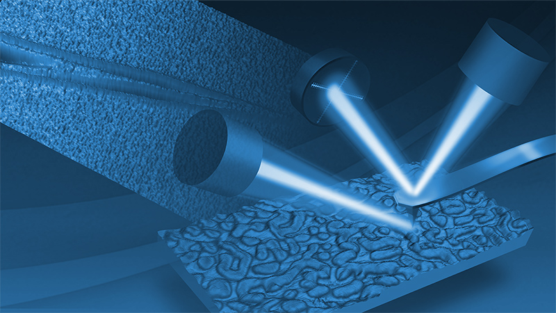
Breaking the Optical Diffraction Limit with SPM: an Overview of nanoIR Capabilities
As material components and devices become smaller and more complex, the need for nanoscale optical characterization and chemical identification grows rapidly. The diffraction limit traditionally restricts the lateral resolution of optical measurements to approximately half of the wavelength of light-on the order of microns in the mid infrared region-making it challenging to achieve high-resolution chemical analysis. This limitation has spurred a long-standing need for robust techniques that can overcome these constraints and provide detailed nanoscale chemical information. Nanoscale infrared (nanoIR) spectroscopy has significantly enhanced our ability to study the chemical properties of materials at the molecular level, and a number of techniques have been developed to conquer the diffraction limit. Three of the main SPM coupled nanoscale IR techniques are photothermal AFM-IR, photoinduced force microscopy (PiFM) and scattering-type scanning near-field optical microscopy (s-SNOM). However, significant ambiguities remain regarding their detection mechanisms and which technique is optimal for a specific application, leaving room for continuous efforts and further discovery. This presentation aims to provide a comprehensive introduction to these three prominent techniques. We will discuss the unique advantages each method offers, and their contrast mechanisms, as well as the respective limitations, including sample preparation and the complexity of data interpretation. A key objective is to resolve common ambiguities in the terminology associated with these techniques, fostering a clearer understanding and providing a common language for researchers in the field. Applications beyond the infrared range will also be explored. By addressing these nuances, we aim to enable a more precise comparison of the methods and encourage their effective application across a wide range of scientific disciplines. This talk will offer attendees a solid foundation to better navigate the diverse nanoIR landscape, facilitating informed decisions about which technique best suits their research needs.
Session Title: SPMConnect: Novel Methods
Date: Tuesday, June 10 th | 3:00 pm
Authors/Presenters: C.A. Phillips, Q. Hu, C. Li, P. De Wolf
Keywords: nanoIR, SPM, AFM, AFM-IR, s-SNOM, nanoscale infrared spectroscopy
Speaker
Cassandra Phillips, Ph.D.
Application Scientist, BrukerCassandra did her Ph.D. at the University of Toronto exploring the photophysics of boron nitride nanotubes using scattering scanning nearfield optical microscopy (s-SNOM) and computational models. She has been working at Bruker Nano Surfaces and Metrology since September 2019 as an Applications Scientist focusing on nanoscale IR spectro-microscopy and other correlated imaging techniques realized with atomic force microscopy.
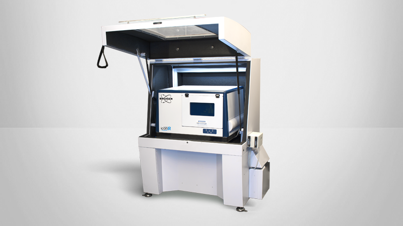
Learn More About the new Dimension Nexus
Dimension Nexus™ delivers an ideal combination of data quality, experiment flexibility, and ease of use in a small-footprint system. It incorporates the milestone innovations of Bruker's NanoScope® 6 controller, PeakForce Tapping® technology, and ScanAsyst® Plus self-optimizing imaging software to deliver more functionality than competing systems in its class. Suitable for both routine and custom experiments and easily upgradable in the field, Dimension Nexus is both an excellent starter system and a perfect addition to any thriving AFM lab.
Featured Products and Technology
Related Links
Thank you
Your request was successfully sent.
You can email us with more information at productinfo@bruker.com.
If you would like to connect with a Bruker representative immediately, here are our regional offices:
Asia: +65 6540 4388
China: +86 10 5833 3000
Europe: +33 172 86 61 00
Japan: +81 3 3523-6361
North America: +1 805-967-1400