10nm Resolution Chemical Imaging with Tapping AFM-IR
Experience High-Resolution Photothermal AFM-IR
During this webinar, two experts in the technique of nanoscale IR spectroscopy in the AFM (AFM-IR) describe the fundamentals of AFM-IR and how and where it is used.
AFM-IR is used for chemical imaging and spectroscopy at the nanoscale.
- Recent improvements have improved the technique’s speed, resolution, and sensitivity.
- Applications for AFM-IR can be found in materials science, life sciences, and polymers research.
- Tapping AFM-IR™ enables testing of softer samples, and at resolutions down to 10 nm.
Webinar Summary
AFM-IR provides chemical imaging and spectroscopy at the nanoscale with recent improvements in speed, resolution, and sensitivity.
In this webinar, the presenters discuss the AFM-IR technique for chemical imaging and spectroscopy at the nanoscale with 10 nm spatial resolution. Craig Prater, Ph.D., introduces the technique, and Kevin Kjoller, Ph.D. presents applications examples.
During the first part of the webinar, Dr. Prater covers the following:
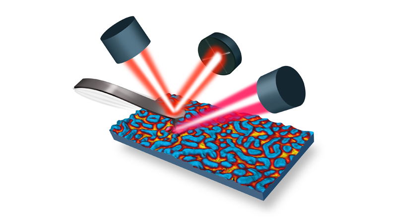
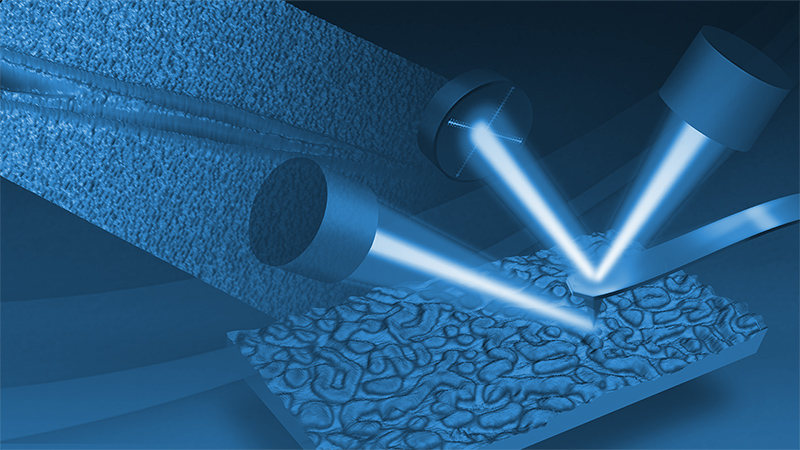
- An introduction to AFM-IR and its ability to overcome the diffraction limit of conventional infrared spectroscopy. AFM-IR works by detecting the thermal expansion of a sample when infrared light is absorbed, which causes an impulse force on the AFM tip.
- Recent innovations that have improved AFM-IR's spatial resolution, measurement speed, and sensitivity, including FASTspectra™ and hyperspectral imaging modes.
During the first part of the webinar, Dr. Kjoller presents various applications of AFM-IR in material science, life sciences, and polymer research. He also describes complementary techniques like nano thermal analysis, scattering SNOM, and fast mapping AFM-IR.
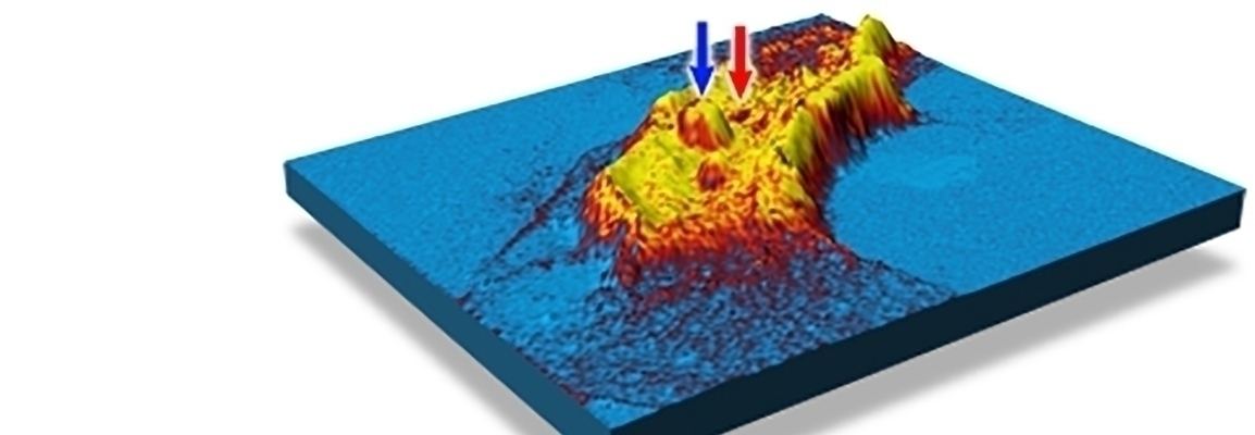
Finally, Dr. Prater describes Tapping AFM-IR, a new mode that allows for softer samples and higher resolution down to 10 nm. Tapping AFM-IR works by oscillating the AFM tip and pulsing the infrared laser asynchronously. This provides chemical contrast that is insensitive to long range background forces.
Find out more about the technology featured in this webinar or our other solutions for nano-IR:
Q&A Session
Note that some Q&A responses in our older webinars may not reflect current offerings. Check out our latest capabilities at Nanoscale Infrared Spectrometers | Bruker.
- What is the range that can be covered by the infrared sources?
- Can existing systems be upgraded to take advantage of the FASTspectra technology?
- How long does it take to collect an IR image with FASTspectra compared to the previous OPO laser?
- Is Tapping AFM-IR used to obtain only images or spectra as well?
- What is the focus size of the infrared laser?
- Do you consider AFM-IR complementary to scanning X-ray microscopy?
- What is the highest temperature possible with nano thermal analysis?
- What is the probe depth of AFM-IR?
- How many composition maps taken at different frequencies can you combine together?
Featured Products and Technology
Speakers

Dr. Craig Prater
Chief Technology Officer, Photothermal Spectroscopy Corp

Kevin Kjoller
VP of Product Development, Bruker Anasys Instruments