EDS on the Nanoscale in TEM/STEM and SEM
EDS on the Nanoscale in TEM-STEM & SEM
In this webinar we highlight the pros and trade-offs for various combinations of EDS instrumentation with different types of electron microscopes for element analysis on the nanoscale.
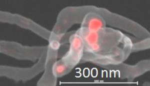
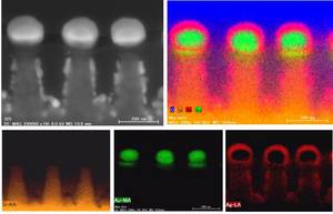
Element mapping with nm-resolution can be routinely achieved in TEM/STEM. Atomic level element ID of light elements in complex samples is possible using EDS in spherical aberration corrected high brightness STEM.
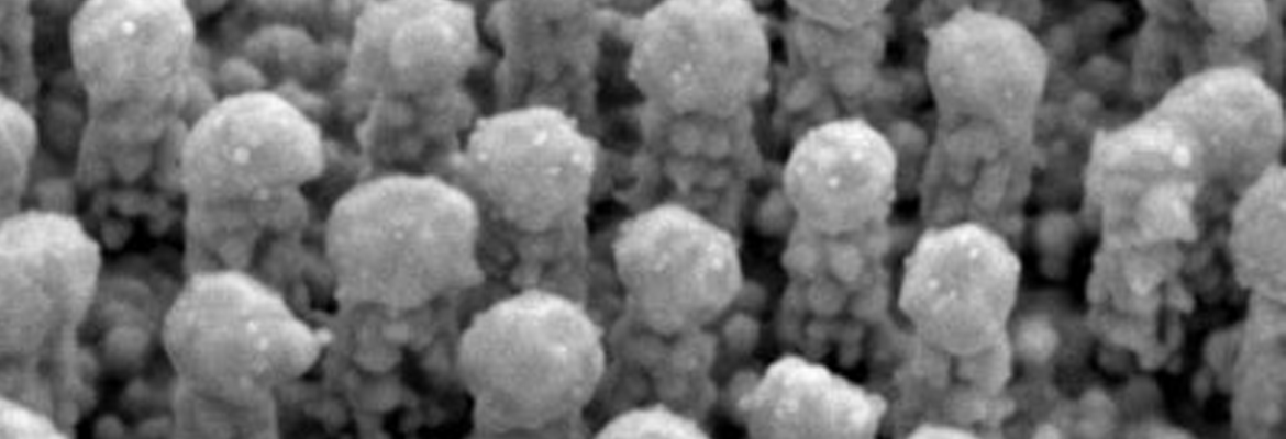
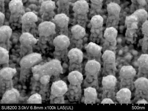
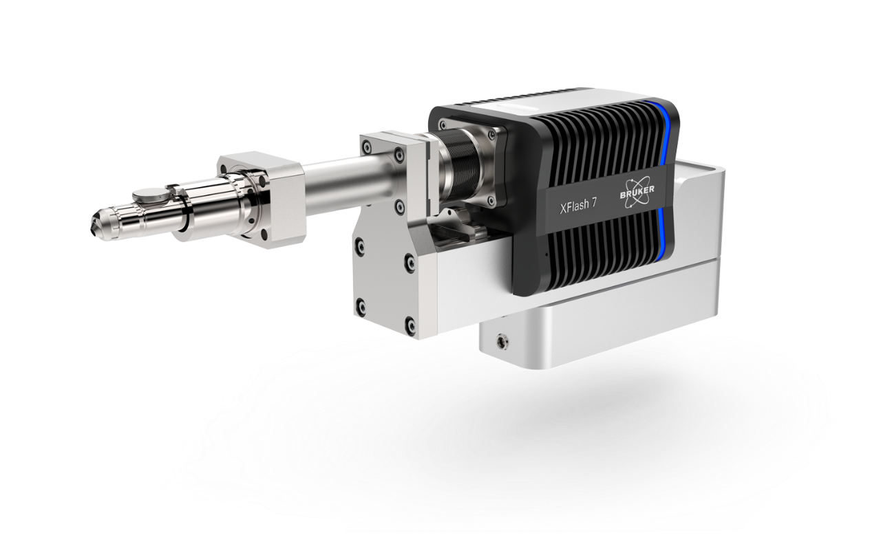
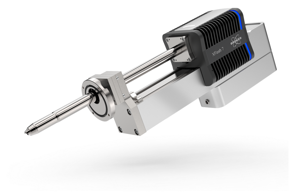
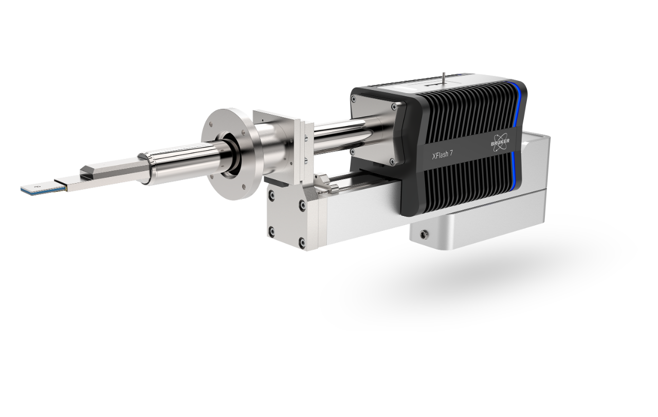
In case of SEM low voltage or electron transparent samples investigated with high solid angle EDS enable qualitative and quantitative element analysis with nm-resolution. In addition EDS analysis at low beam currents useful for beam sensitive and charging materials will be demonstrated. High solid angle EDS can be provided by multiple detector systems or the annular XFlash® Flat Quad. The annular detector has the additional advantage of a high take-off angle beneficial in case of high sample topography.
Examples from materials and life science will be used to show acquisition approaches and explain qualitative and quantitative data analysis using ESPRIT software features. Quantification procedures for thin samples based on the Cliff-Lorimer and the Zeta-factor-method will be explained. Furthermore EDS using the annular quad detector in SEM will be discussed.
The webinar will be round off by a 15-minute Q&A session where our experts will answer your questions.
Who Should Attend?
- Scientists, engineers, students using EDS on SEM and TEM/STEM
- Researchers in materials and life science interested in element distribution on the nanoscale
Speakers

Dr. Meiken Falke
Global Product Manager EDS/TEM, Bruker Nano Analytics

Dr. Igor Németh
Application Scientist EDS, Bruker Nano Analytics
Mats Eriksson
Department Manager, Hitachi High-Technologies
Watch this Webinar On-Demand
Please enter your details below to gain on-demand access to this webinar.