
Analytical Alternatives to WDS for Elemental Analysis on SEM
Solving WDS Applications with Windowless EDS and micro-XRF on SEM
Many researchers use Wavelength Dispersive Spectroscopy (WDS) to overcome challenges such as elemental peak overlaps, low signal intensities or to perform analysis at low kV.
Developments in EDS peak deconvolution routines in conjunction with modern windowless detectors and micro-XRF on SEM now mean that these challenges can be overcome without the disadvantages of WDS analysis.
Continue reading to find out about light element detection & peak deconvolution, as well as trace element detection & X-ray line separation using alternative SEM-based analysis technologies.
Overcoming the Limitations of Wavelength Dispersive Spectroscopy
Wavelength Dispersive Spectroscopy (WDS) is a long-established and highly trusted analytical technique in materials characterization.
WDS provides outstanding spectral resolution, enabling the reliable separation of overlapping peaks and precise elemental identification, even in complex sample matrices. Additionally, it provides a very high peak to background ratio, enabling the detection of overlapping elements present at low concentration levels. WDS based on a parallel beam optic additionally serves a strong light element efficiency making it the preferred choice for low acceleration voltage and low probe current for various applications fields.
However, these performance advantages come with considerable constraints. WDS acquires spectra sequentially, which fundamentally limits measurement speed compared with the simultaneous full‑spectrum acquisition of energy‑dispersive X‑ray detectors (EDS). In addition, WDS requires substantial user expertise to maintain optimal instrument alignment, select appropriate standards, and perform accurate quantification since the technique is intrinsically standards‑based and cannot operate in a standardless mode.
Modern windowless EDS detectors combined with a micro‑XRF source overcome the typical limitations of WDS and still deliver high analytical performance. This integrated approach offers a powerful, flexible, and cost‑efficient alternative for both routine and advanced materials analysis. It supports rapid, high‑throughput elemental mapping and full‑spectrum acquisition, with strong analytical sensitivity from micro‑XRF excitation and excellent light‑element detection from windowless EDS. Both technologies can be seamlessly integrated into existing SEM platforms and require far less calibration, alignment, and maintenance than WDS. They also support standardless quantification and eliminate consumables such as flow counter gases.
Light Element Detection & Peak Deconvolution
By removing the detector window, absorption of low energy X-rays is drastically reduced, resulting in considerably enhanced sensitivity for light and ultra‑light elements.
When combined with modern multi‑segment detector architectures, large solid angles, and high count‑rate capability, windowless EDS delivers substantial gains in efficiency: typically, up to a factor of 3 for light elements and up to 16 for ultra‑light elements such as beryllium, when compared with conventional EDS systems.
In addition, simultaneous full‑spectrum acquisition enables fast measurements even at low accelerating voltages and beam currents. This makes windowless EDS an excellent choice for the analysis of beam‑sensitive material and high‑speed elemental mapping, as well as routine workflows where both throughput and accuracy are important.
Bruker has more than 20 years of experience and know-how in individual detector calibration and EDS peak deconvolution routines.
Windowless EDS vs. WDS for the Analysis of TaSi2
In this TaSi₂ sample containing inclusions of Si, separating Ta from Si can be challenging due to the small 28 eV offset between the energetic positions of the main SI-K and Ta-M lines.
While WDS can physically resolve overlapping peaks, modern EDS deconvolution routines can also separate Ta from Si but much more quickly. What takes minutes with WDS takes seconds with EDS.
EDS Spectrum Deconvoultion vs. WDS Spectrum Resolution for TaSi2


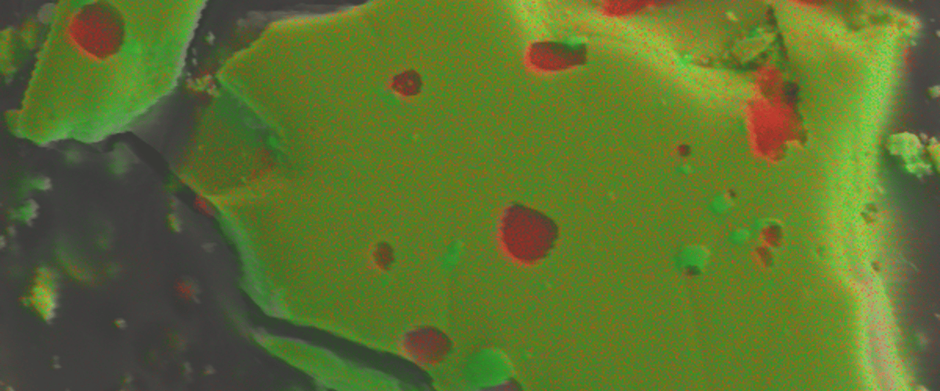
EDS Map vs. WDS Map for TaSi2


The Light Element Performance of WDS, Without the Complexity
Using our QUANTAX EDS analytical system with the XFlash® 7100oval windowless EDS detector the elemental analysis and mapping of even light and ultra-light elements is possible in less time than it would take to perform WDS analysis.
If you are interested in learning more about the benefits of our windowless EDS detectors for your application contact a Bruker expert.

Trace Element Detection & Separation of X-ray Line Series
Micro‑XRF on SEM combines efficient X‑ray excitation with simultaneous EDS spectral acquisition. This results in high sensitivity and a very low spectral background, enabling dependable trace‑element detection down to the lower ppm range.
Micro-XRF on SEM is most efficient for the mid- and higher elemental range and can therefore excite higher energy K- and L-lines more efficiently. These regions typically show far fewer peak overlaps than the low‑energy range. As a result, the ultra‑high spectral resolution traditionally associated with WDS is often not required for many applications. At the same time, the ability to excite the full X‑ray spectrum and observe multiple line families increases confidence that an element is truly present in the sample.
Trace Element Detection with Micro-XRF on SEM
Detecting trace elements at the tens-of-ppm level can be challenging with conventional EDS. For example, NiO at 20 ppm and HfO2 at 40 ppm in glass may remain undetected because their weak characteristic signals are buried within the spectral background.
The superior sensitivity of micro-XRF on SEM, using the XTrace 2 micro-XRF source, enables the clear identification and analysis of these trace elements, extending the detection capabilities of SEM-based elemental characterization.

Separation of X-ray Line Series in the High-Energy Range with Micro-XRF on SEM
Rare Earth Elements (REEs) frequently occur together in mineral samples, such as La, Ce, and Pr, resulting in severe peak overlaps in the low-energy region of conventional EDS spectra.
With the addition of XTrace 2 to the SEM, high-energy X-ray line families are visible even beyond 40 keV (e.g., the Nb Kβ line shown in the figure). In this high-energy range, the characteristic lines of individual REEs are well separated, eliminating the overlapping of peaks and enabling confident identification of rare earth elements, even at trace concentration levels.

High-Throughput Trace Element Mapping
Using QUANTAX Micro-XRF with XTrace 2 the analysis and mapping of trace elements, and detection of separated X-ray lines, is possible in significantly less time than WDS analysis.
If you are interested in learning more about the benefits of micro-XRF on SEM for your application contact a Bruker expert.

Enhance Your Analysis with Combined micro-XRF and EDS on SEM
Windowless EDS and micro-XRF complement each other and directly address key limitations of conventional WDS systems.
Together, they provide faster, more efficient, and more cost‑effective elemental analysis, delivering excellent sensitivity for both light‑element detection and trace‑element quantification.
Systems and detectors used:
- Windowless EDS with the XFlash® 7100oval EDS detector, as part of QUANTAX EDS.
- Micro-XRF on SEM with the XTrace 2 secondary X-ray source, as part of QUANTAX Micro-XRF.
Contact a Bruker Expert
If you are interested in learning more about our alternatives to WDS or how Bruker's detectors can benefit your application contact a Bruker expert.