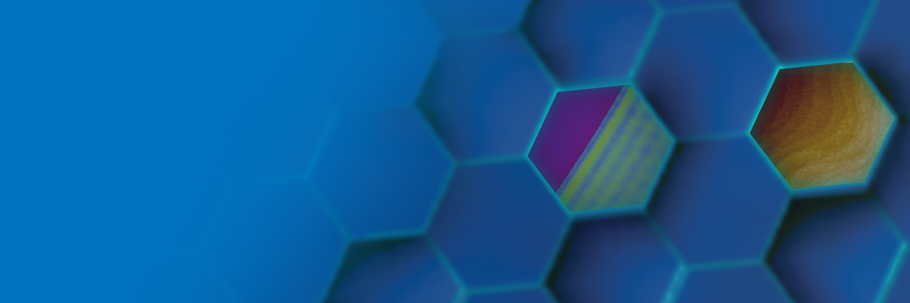

Advances in AFM for the Characterization of 2D Materials
Comprehensive nanoscale characterization of 2D materials using AFM
Characterizing 2D materials involves examining a wide range of nanoscale structures, properties, and chemistry. Atomic force microscopy (AFM) is extremely versatile, making it ideal for addressing these complexities. With AFM, researchers can investigate various aspects of 2D materials (often simultaneously), gaining detailed insights that are essential for advanced applications.
Join us for this webinar to learn about:
- Single-platform correlation of structure, properties, and chemistry
- Commonly used AFM modes for 2D materials characterization
- Manipulation modes for in-situ device fabrication by cutting, folding, or oxidation
Webinar Summary
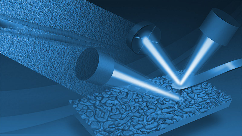
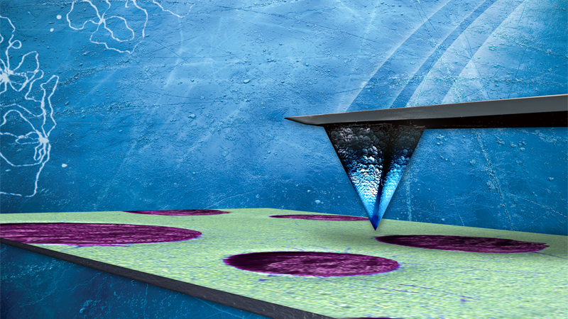
AFM plays a pivotal role in the nanoscale characterization of 2D materials by providing high-resolution topographical, mechanical, and electrical property mapping at the nanoscale, down to the atomic level. Identifying and characterizing single layers and multilayers is routine, while crystal orientation can often be determined with the proper choice of mode and probe. Since the AFM probe can act as a nanoscale electrode, it is possible to directly measure electrical properties of these materials at the relevant length scales between 1 and 100 nm. Photothermal AFM-IR (AFM-IR) adds localized chemical identification with nanometer scale spatial mapping by integrating infrared spectroscopy with AFM. Together, these capabilities correlate structure and chemistry, enabling comprehensive studies of complex 2D material systems. The AFM probe can also be used for nanomanipulation and nanolithography, allowing device fabrication by cutting, folding, or oxidation.
In this webinar, we discuss:
- Commonly used AFM modes for identification and characterization of 2D materials
- Recent advancements in consistency of high-resolution 2D material mapping
- Characterization of nanoelectrical properties in 2D materials through conductivity, impedance, and surface potential measurements
- Nanoscale chemical identification through AFM-IR spectroscopy and mapping
- Nanolithography on 2D materials, for example by tip-induced local anodic oxidation
Find out more about the technology featured in this webinar or our other solutions for AFM:

Bruker Speakers
Bede Pittenger, Ph.D., Sr. Staff Development Scientist, AFM Applications, Bruker Nano Surfaces
Dr. Bede Pittenger is a Senior Staff Development Scientist in the AFM Unit of Bruker's Nano Surfaces Business. He received his PhD in Physics from the University of Washington (Seattle, WA) in 2000, but has worked with scanning probe microscopes for 25 years, building systems, developing techniques, and studying properties of materials at the nanoscale. His work includes more than thirty publications and three patents on various techniques and applications of scanning probe microscopy. Dr. Pittenger's interests span topics from interfacial melting of ice, to mechanobiology of cells and tissues, to the nanomechanics of polymers and composites.

Ming Ye, Ph.D., Applications Scientist, Bruker
Dr. Ming brings over 20 years of extensive experience in the field of Atomic Force Microscopy (AFM) and microanalysis, currently serving as an Application Scientist within the Bruker North America team. After earning a Ph.D. from the Chinese Academy of Sciences in 2010, Dr. Ming conducted advanced postdoctoral research at the Max Planck Institute. The journey into the commercial AFM sector began in 2013 in Berlin, where Dr. Ming joined JPK Instruments AG—the predecessor to Bruker BioAFM. Prior to the current role at Bruker NA, Dr. Ming served as the Principal Scientist for Microanalysis at BASF Asia Pacific, bridging the gap between fundamental research and large-scale industrial solutions.

Peter De Wolf, Ph.D., Director of Technology & Application Development
Peter De Wolf is director for AFM technology & application development at Bruker Nano Surfaces, covering all applications related to Scanning Probe Microscopy (SPM). He obtained his PhD from IMEC, Belgium on the development of new SPM methods for 2D carrier profiling in semiconductors and has more than 25 years of experience on SPM. He is the author and co-author of over 30 publications related to electrical characterization using SPM. He also owns several SPM patents, and developed several new SPM modes for electrical characterization.