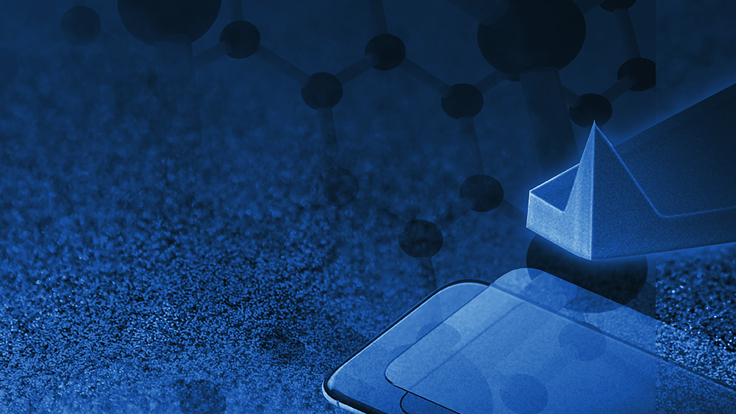

Advances in AFM for the Characterization of 2D Materials
Comprehensive nanoscale characterization of 2D materials using AFM
Characterizing 2D materials involves examining a wide range of nanoscale structures, properties, and chemistry. Atomic force microscopy (AFM) is extremely versatile, making it ideal for addressing these complexities. With AFM, researchers can investigate various aspects of 2D materials (often simultaneously), gaining detailed insights that are essential for advanced applications.
Join us for this webinar to learn about:
- Single-platform correlation of structure, properties, and chemistry
- Commonly used AFM modes for 2D materials characterization
- Manipulation modes for in-situ device fabrication by cutting, folding, or oxidation
Webinar Summary
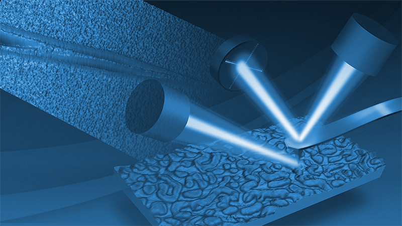
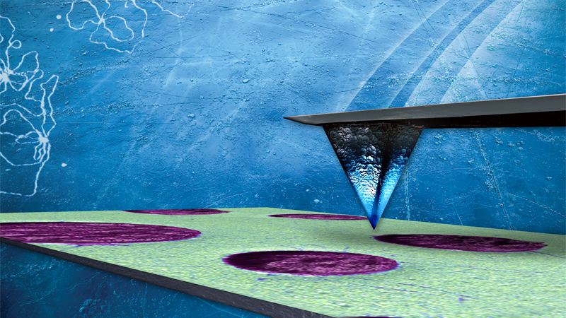
AFM plays a pivotal role in the nanoscale characterization of 2D materials by providing high-resolution topographical, mechanical, and electrical property mapping at the nanoscale, down to the atomic level. Identifying and characterizing single layers and multilayers is routine, while crystal orientation can often be determined with the proper choice of mode and probe. Since the AFM probe can act as a nanoscale electrode, it is possible to directly measure electrical properties of these materials at the relevant length scales between 1 and 100 nm. Photothermal AFM-IR (AFM-IR) adds localized chemical identification with nanometer scale spatial mapping by integrating infrared spectroscopy with AFM. Together, these capabilities correlate structure and chemistry, enabling comprehensive studies of complex 2D material systems. The AFM probe can also be used for nanomanipulation and nanolithography, allowing device fabrication by cutting, folding, or oxidation.
In this webinar, we discuss:
- Commonly used AFM modes for identification and characterization of 2D materials
- Recent advancements in consistency of high-resolution 2D material mapping
- Characterization of nanoelectrical properties in 2D materials through conductivity, impedance, and surface potential measurements
- Nanoscale chemical identification through AFM-IR spectroscopy and mapping
- Nanolithography on 2D materials, for example by tip-induced local anodic oxidation
Find out more about the technology featured in this webinar or our other solutions for AFM: