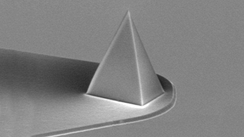
Dimension 2D AFM
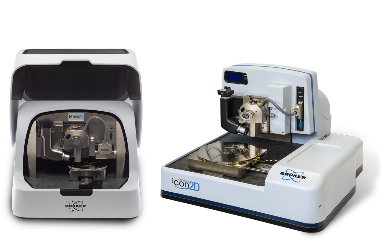
Dimension 2D AFMs
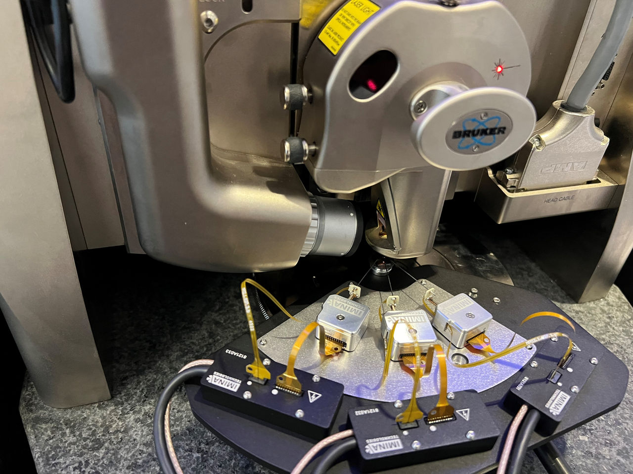
Dimension 2D systems combine Bruker’s proven, industry-leading AFM platforms with a curated suite of highest-priority modes and capabilities to meet the critical requirements of modern 2D materials research.
These turnkey systems maintain ultimate stability for up to atomic defect resolution. Motorized staging streamlines flake-finding, stitched optical overviews, automated imaging routines, and large-area surface cleaning or smoothing. An open-access, large-sample, tip-scanning instrument design enables cutting-edge experiments from in-situ device testing to quantum twisting microscope (QTM) integration.
For advanced research requiring additional modes, capabilities, or environmental control, Dimension 2D is a scalable and future-proof solution. It offers customizable configurations, access to an expansive library of additional modes, and expert support that will help your 2D materials research run smoothly.
Workflow-Ready Solution for 2D Materials Research
Key capabilities and components
-
Superior Performance
-
High-Resolution Imaging
-
Fragile-Sample Protection
-
Advanced Environmental Control
-
Rapid Flake-Finding and -Targeting
-
Multimodal Property Mapping
-
Versatile Sample Modification
-
Effective Cleaning and Smoothing
High-Performance AFMs
Dimension 2D systems are designed, built, and verified for superior performance. Central to their best-in-class capabilities is a unique combination of cutting-edge hardware, software, and accessories.

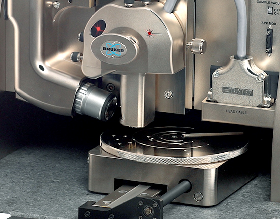
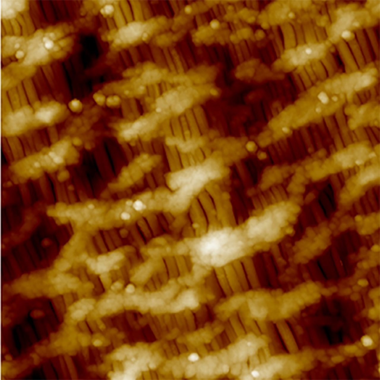

Advanced Modes and Ultra-Stable Design
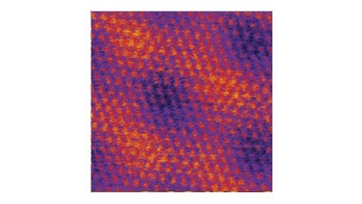
Dimension 2D systems enable reproducible imaging from the microscale down to lattice‑ and atomic‑level features that can confidently be used for quantitative nanometrology (e.g., thickness, twist angle, and lattice constant measurements).

Control of Imaging Forces and Atmosphere
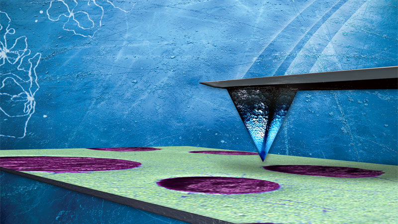
Dimension 2D systems protect fragile monolayers, suspended films, and loosely adhered flakes by precisely controlling tip–sample interaction. minimizing applied forces, and offering optional atmosphere control.
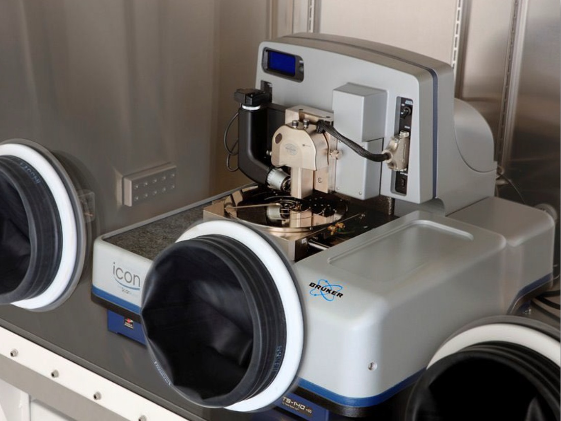
Controlled-Environment Configurations
Dimension 2D systems maintain high stability and imaging performance even with configurations including a glovebox or temperature control.

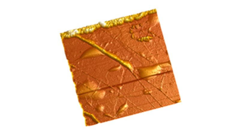
Repeatable Flake‑Finding and Navigation
Dimension 2D systems enable efficient searching and targeting across large or multiple samples.
Structure, Property and Functional Response Correlation
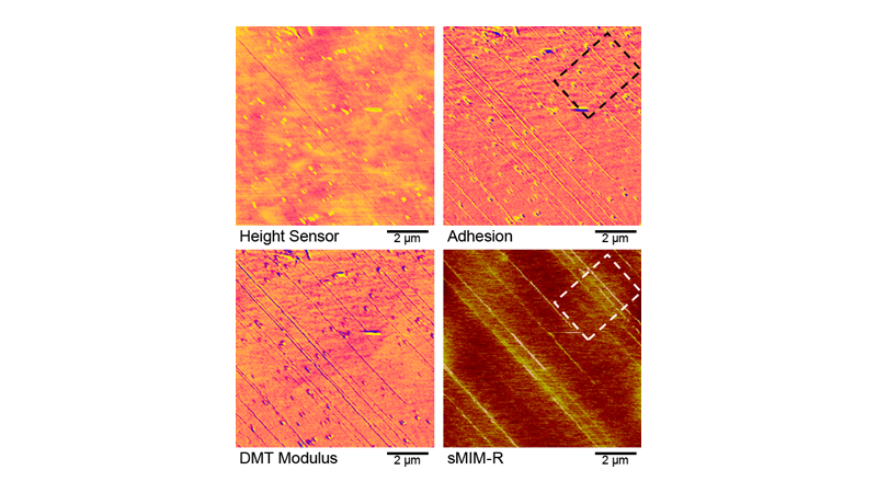
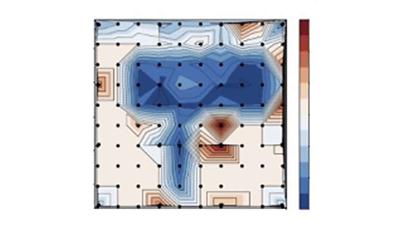
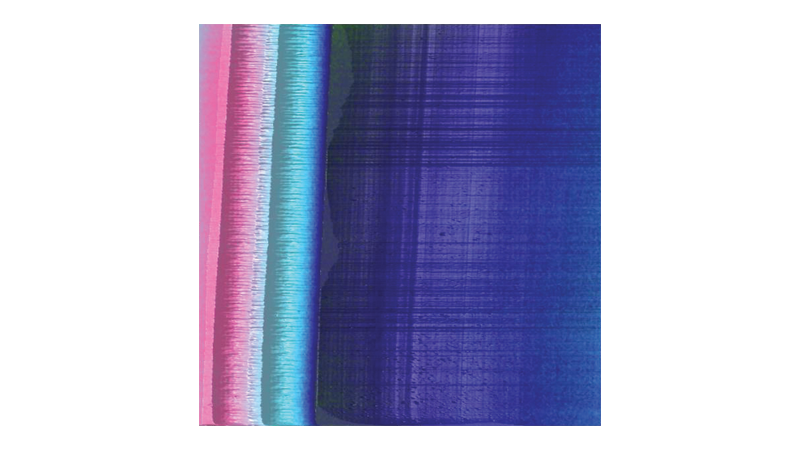
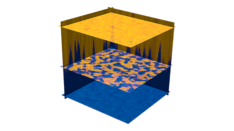
Dimension 2D systems capture co‑registered datasets that enable the correlation of structure to local properties and functional response. Below is a selection of important AFM modes for structure–property–response correlations in 2D materials research.
Nanolithography and Nanomanipulation
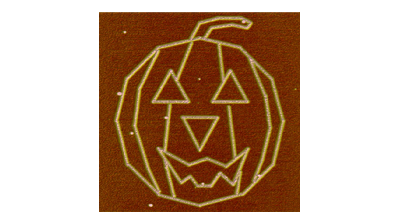
Dimension 2D systems extend AFM beyond measurement to enable direct cutting, folding, or modification of 2D materials through controlled tip-sample interaction.
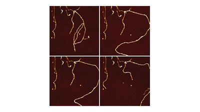
Surface Cleaning and Smoothing
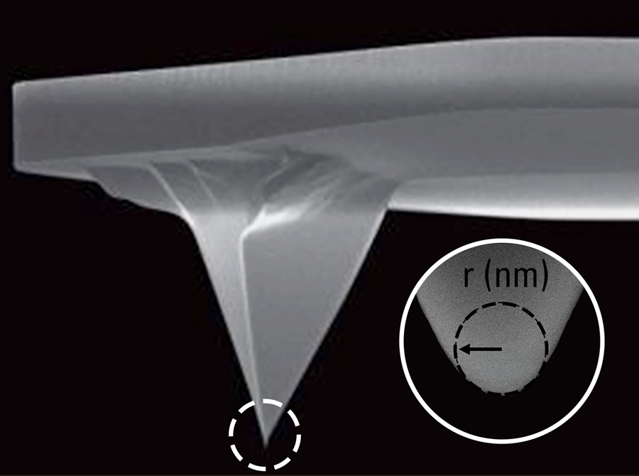
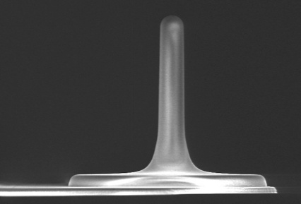
Dimension 2D systems streamline the processes of removing contamination and bubbles from areas of interest.
Comprehensive Library of 2D Materials‑Optimized Modes
Dimension 2D systems integrate an application‑tailored library of AFM modes that provide access to the contrast mechanisms and signal sensitivity needed to characterize structure, properties, and interfaces of 2D materials.
Only Dimension 2D provides:
A turnkey suite of essential AFM modes for high‑resolution imaging and nanomechanical testing
Access to multiple contrast mechanisms, including electrical, mechanical, lateral force, and tunneling interactions
An extensive catalog of optional modes and capabilities for advanced and specialized measurements
Maximum Flexibility for Advanced and Complex Experiments
Dimension 2D systems accommodate evolving research needs, non‑standard configurations, and complex experimental setups without compromising performance.
Only Dimension 2D offers:
An open‑access, tip‑scanning platform architecture compatible with advanced techniques such as quantum twisting microscope (QTM) integration
Support for environmentally controlled and non‑standard experimental conditions within the same platform
The ability to extend the system with additional modes, capabilities, and accessories as research requirements evolve

Fastest Path from Sample to Data
Dimension 2D systems are configured to streamline the full measurement workflow—from locating flakes to acquiring and analyzing data.
Only Dimension 2D provides:
Large motorized stage for rapid navigation, multi‑site measurements, and large‑area mapping
Large-area optical images with addressable coordinates, enabling fast targeting and reliable return‑to‑location imaging
API-driven workflows for rapid, consistent, and repeatable data acquisition
Integrated data capture and handling, including hyperspectral acquisition and batch analysis workflows
Dimension 2D AFM: Proven Impact in Real Research Applications
From flake characterization to multimodal functional analysis, Dimension 2D AFMs enable real‑world experiments that link structure, properties, and device performance.


Enhanced Contrast: Visualizing moire pattern formed by hBN layer on graphene
Torsional force microscopy (TFM), recently developed by Bruker, provides highest‑resolution imaging of 2D materials via enhanced lateral‑force sensitivity — including visualization of moiré superlattices in van der Waals heterostructures.
In this example, TFM resolves the 2.6 nm moiré pattern produced by the graphene/hBN twist and the underlying 0.246 nm atomic lattice of the graphene in a single image. Adjusting load in the same mode pulls contrast from layers beneath the top film.
Read more about TFM in the original journal article or our application note on torsional resonance modes.

Gentle Imaging: Resolving graphene membrane over open pore
PeakForce Tapping® is Bruker’s proprietary technology for controlling peak normal force directly at every pixel — essential for fragile monolayers and suspended films.
This example shows graphene suspended across an open pore. Where TappingMode produced unusable noise in the image, PeakForce Tapping resolves the membrane cleanly.
Learn more in this webinar, where we asked our experts to talk about their favorite PeakForce Tapping modes.

Co-registered Property Mapping: Distinguishing artifacts in epitaxial graphene on SiC
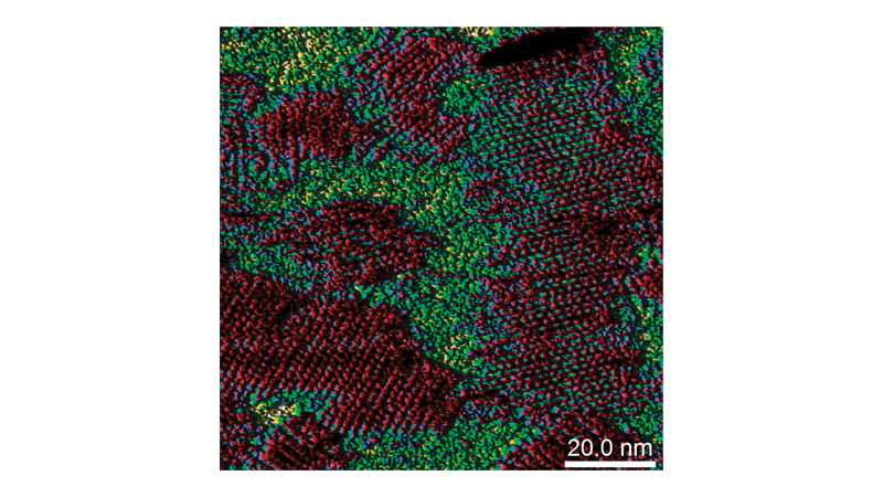
PeakForce QNM® extracts adhesion, deformation, and stiffness from each PeakForce Tapping force curve. PeakForce TUNA® adds a current channel under applied bias, producing co‑registered mechanical and electrical maps from the same force–distance curve.
In this example, a multimodal dataset was used to distinguish artifacts from real material changes in epitaxial graphene on SiC. Modulus and adhesion mapped coverage directly, and with a bias applied, the current channel reproduced the same pattern in conductivity contrast.
Hear more about this dataset during the 2D materials section of this webinar.

Surface Potential and Work-Function Contrast: Understanding image contrast
Kelvin probe force microscopy (KPFM) measures the tip–sample contact potential difference, yielding layer-resolved work function and charge maps on graphene, TMDs, and hBN. Bruker's KPFM family spans AM-, FM-, and HV-KPFM for gated devices, plus PeakForce KPFM for lowest-force surface potential on fragile flakes.
In this example showing mechanically exfoliated multilayer graphene on silicon oxide, KPFM and Raman were used together to understand the true origins of image contrast. After cross-checking, the D-band feature here was traced back to mechanical folding rather than dismissed as a Raman artifact.

Subsurface and Dielectric Imaging: Resolving electrical contrast on buried devices under hBN
Kelvin Scanning microwave impedance microscopy (sMIM) reads the tip–sample impedance at microwave frequency, recovering capacitive and resistive channels that surface-only electrical modes cannot. PeakForce sMIM adds force-controlled engagement for repeatable measurements on soft or loosely adhered samples.
This example shows electrical contrast on buried device structures under hBN. The capacitive channel resolves buried lines and the gaps between them, with the 70 nm nominal gap broadening to ~200 nm FWHM, consistent with subsurface signal spreading through the dielectric.
Hear more about this dataset in this webinar.

Dimension 2D Select Specifications
| XY-Scan Range | 90 μm x 90 μm typical, 85 μm minimum | |
|---|---|---|
| Z-Scan Range | 10 μm typical, 9.5 μm minimum | |
| Sensor Noise | XY-Position Sensor: ≤0.15 nm RMS; Z-Sensor: 35 pm RMS (typical imaging bandwidth ≤625 Hz) | |
| Glovebox Compatibility | Turnkey integrated MBraun solution available; designed for maximum performance of Dimension systems | |
Dimension Icon 2D | Dimension Nexus 2D | |
| Sample Size/Holder | 210 mm vacuum chuck for samples: ≤210 mm diameter, ≤15 mm thick | 150 mm vacuum chuck for samples: ≤150 mm diameter, ≤15 mm thick |
| Motorized Positioning XY-Stage | 180 mm × 150 mm inspectable area; 3 μm repeatability, bidirectional; programmable for multi-site measurements | 150 mm x 150 mm inspectable area; 6 μm repeatability, bidirectional; programmable for multi-site measurements |
| Vertical Noise Floor (typical imaging bandwidth ≤625 Hz) | <30 pm RMS in appropriate environment | ≤40 pm RMS in appropriate environment |
| Acoustic Isolation | Operational in environments ≤85 dBC continuous acoustic noise | Operational in environments with ≤75 dBC continuous acoustic noise |
| Download the brochure for full specs list | ||
Powered by the NanoScope 6 AFM Controller
Featuring higher speeds, lower noise, and greater AFM mode flexibility, the NanoScope 6 controller allows users to harness the full potential of our high-performance Dimension and MultiMode AFM systems. This latest generation controller provides unprecedented accuracy, precision, and versatility for nanoscale surface measurements in every application.
NanoScope 6 uniquely enables Bruker AFMs to:
- Operate in more imaging modes than is possible with competing systems, including unique and advanced AFM modes that require complex control and analysis
- Collect accurate, quantitative data for nanoelectrical and nanomechanical property measurements in every application
- Optimize and customize scanning parameters to meet even the most demanding research and industry measurement requirements
- Provide ultimate ease of use with Bruker’s exclusive ScanAsyst® Plus self-optimizing imaging software with enhanced intelligent algorithms and patent-pending smart functionality (find out if your Bruker AFM is eligible for the free ScanAsyst Plus upgrade here)