
JVSENSUS-600F
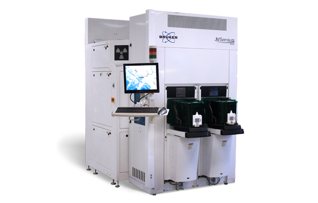
JVSensus-600F
The JVSensus-600F is the X-ray defect metrology system for 300mm Si device manufacturers. It helps identify problems encountered during wafer production using the latest X-ray diffraction imaging (XRDI) technology. Applications include monitoring edge damage to prevent costly wafer breakage during ultra fast anneal. It can qualify and monitor process tools at any technology node, which reduces cycle times and facilitates fab expansion.
Easily Identify Crystalline Defects
JVSensus enables its users to identify cracks and other defects in the wafer which can cause catastrophic structural failure, BEFORE the breakage occurs. Once a defect has been observed, non-destructive cross section review images can be performed to locate the defect locations within the wafer depth.

Measure on Patterned Wafers

Measurements can be performed on blanket, patterned, and metalized wafers without sample preparation. The defects can be identified even when a pattern is present on the wafer.
Detect Slip
The major cause of overlay issues is slip. Whether it's a logic patterned wafer, GaN on Si or ingot slides, JVSensus can detect slip in minutes.

How Can We Help?

Service and Application Support to Optimize Tool Utilization
The decision to invest in high-performance metrology is based on more than instrument performance and price. Bruker is committed to keeping your tool running at the peak of up-time and productivity. We have a highly educated worldwide team of service and support personnel that takes great pride in first-time solution of issues. Our variety of service coverage programs can be customized to match your specific requirements, including optimization of tool performance, recipe writing, and in-person technical support visits.
Bruker tailors services to your needs:
- Priority technical support
- Advance replacement parts and assemblies stored in regional warehouses for rapid response times
- Application and training services