Thin Film Characterization Using Spectroscopic Reflectometry and Ellipsometry Techniques
Discover a one-of-a-kind technology line designed to meet the demands of new and future thin film materials.
This one-hour webinar provides a detailed and methodical explanation of spectroscopic reflectometry and ellipsometry techniques and the use and advantages of polarized light techniques for measuring thin films - specifically films on silicon and today's complex semiconductor devices (multi-layer/multi-stack).
Topics covered in this expert-led discussion include:
- Theoretical fundamentals and respective accuracy and measurement ranges;
- Bruker’s unique algorithms, hardware implementations, and fully automated equipment; and
- Real-life use cases, including both medical device and semiconductor device applications.
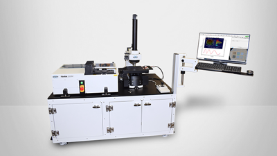
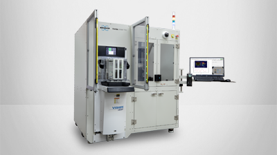
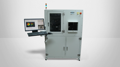
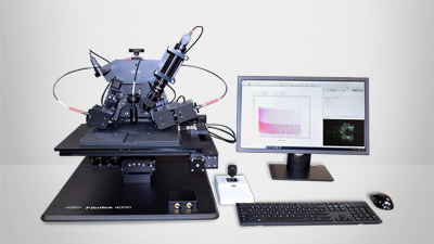
Find out more about the technology featured in this webinar and our industry-leading FilmTek thin film measurement tools:
This webinar is included in our Thin Film Characterization Knowledge Pack.
Webinar Preview
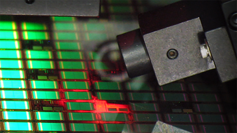
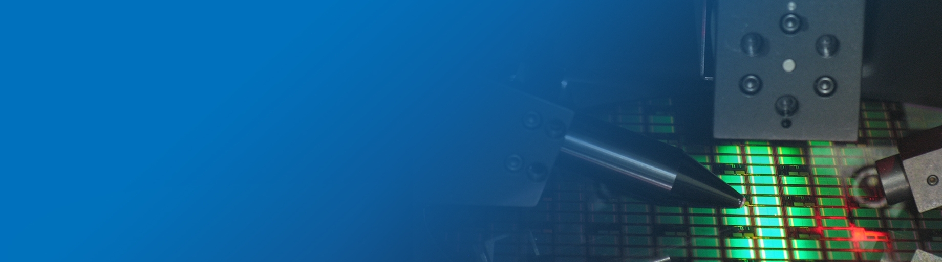
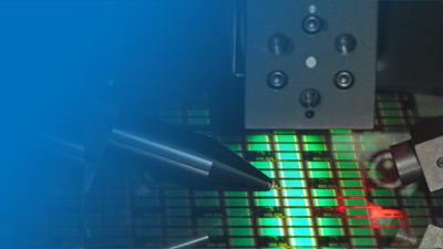
Non-contact optical spectroscopic reflectometry, spectroscopic ellipsometry, and multiple-angle reflectometry technques provide a complementary approach to AFM and profilometry for the complete morphological and optical characterization of single or multi-layer thin films.
Like AFM and profilometry, these techniques operate by directing light at a sample of interest. Change in the reflected intensity or polarization of the light is then modeled to infer physical parameters of interest. Specifically:
- Reflectometry measures the change in the reflected intensity of the light, which depends on the refractive index, extinction coefficient of the film, film thickness, and optical constants of the substrate.
- Ellipsometry measures the change in the polarization of light, which is sensitive to the sample surface and the thickness of very thin films.
Bruker's FilmTek tools enable thin film measurements and analyses that are either inaccessible or unreliable by traditional metrology instruments. Three key technologies enable the unique performance of FilmTek optical metrology tools:
- Multi-angle, differential power spectral density (DPSD) technology for high-resolution refractive index measurements
- Multi-angle, differential polarimetry (MADP) technology for thin film and multi-layer measurements
- Small and collimated spot technology for thick film measurements
Additional notable FilmTek features also discussed in this webinar include:
- Rapid measurement of many wavelengths and the resultant generation of more data points than unknowns;
- Utilization of different measurement heads depending on the required spot size, wavelength range, and measurement type; and
- Automation options designed to meet customer requirements from R&D through high-volume production.
FilmTek tools’ unique combination of proprietary measurement technologies, patented optical design, and proprietary software results in unparalleled optical metrology performance. The speaker demonstrates this performance for production and QA/QC use cases in medical devices and semiconductor devices, including using:
- FilmTek 2000M to enable the manufacture of implantable glucose sensors for diabetes patients by monitoring film thickness.
- FilmTek 2000 PAR-SE to support the manufacture of single use Blood sensors (which include thin films and multi-layer stacks) by monitoring film thickness.
- FilmTek 2000M TSV and thick film technology for the measurement of trench depth for 60 µm-deep trench structures and the thickness measurement of 100 µm silicon on a bonded device wafer.
- FilmTek 4000 for the measurement of refractive index versus temperature of a silicon oxide film.
- FilmTek 2000M TSV for the measurement of individual TSV depth and CD for vias that were 4.5 µm in diameter and 70 µm deep — dynamic repeatability for the head depth was better than 2 nm, and the CD dynamic repeatability was 20 nm.
The presenter also answers questions from the audience about specific capabilities, sample compatibility, and product selection. Among the answered questions were:
- What is the minimum thickness detectable?
- How easy is it to use the simulation to extract the information?
- Do you offer options for users to analyze or optimize models offline?
- Can metal films be measured with FilmTek tools?
- Can films on metal mesh be measured?
- Can transparent polymer film thickness be measured?
- Which instrument would be best suited for multi-layer films (2-500 µm)?
- Which FilmTek models are turnkey solutions?