
Full Range EDS Analysis of Non-Conductive Samples in the SEM by the Addition of micro-XRF
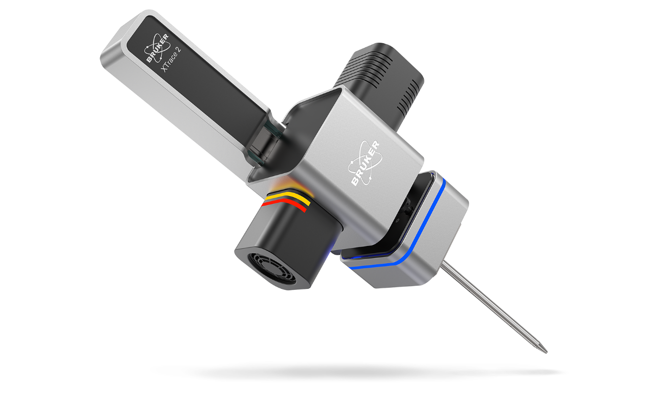
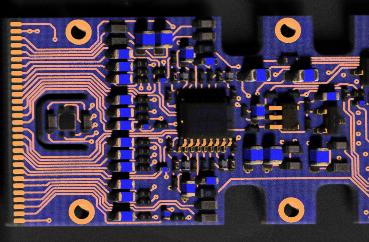
We will present case studies involving unprepared samples and explore the extended range of elemental information accessible through Full Range EDS capabilities. This full range covers two sources: the SEM electron beam (e-beam) and the photon beam from the micro-XRF source, our latest XTrace 2. As a complementary analytical technique, micro-XRF on SEM simplifies sample preparation and is even effective for analyzing samples with irregular or rough surfaces. This makes it an ideal solution for spatially resolved sample analysis on large, diverse samples, while achieving micrometer resolution.
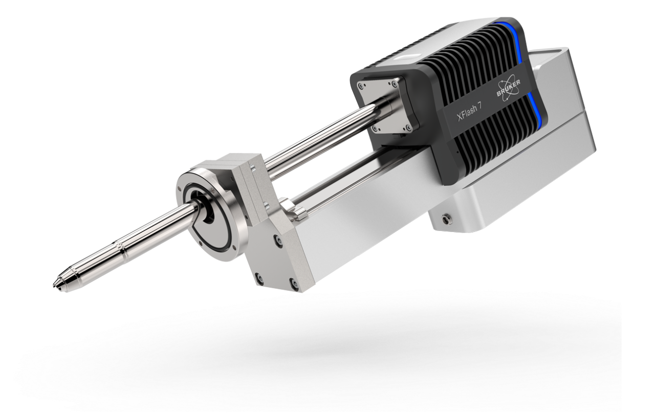
Additionally, we will demonstrate how to bridge sample information from the centimeter scale down to the micrometer scale in the SEM by using the Full Range EDS concept based on our XFlash® 7 EDS detector. Our discussion will include examples of unpolished and uncoated samples, such as topographically complex, highly charging, and multi-layered specimens, showcasing the system's precision and versatility across a wide variety of materials.
Who Should Watch?
Scientists and researchers interested in EDS/micro-XRF technologies for SEM
Experienced professionals managing resources in electron microscopy labs.
Speakers
Dr. Yang Yang
Application Scientist - micro-XRF on SEM and EDS, Bruker Electron Microscope Analyzers
Stephan Boehm
Product Manager - micro-XRF on SEM and WDS, Bruker Electron Microscope Analyzers
Watch this Webinar On-Demand
Please enter your details below to gain on-demand access to this webinar.
