EBSDによるマイクロプロセッサ用ワイヤボンディング部の微細組織評価

Ball bonding is a type of wire bonding commonly used for electrical interconnections in semiconductor devices. A weld is created between the gold ball and the surface of the chip using heat, static pressure and ultrasonic energy.
Optimum bonding settings are tricky to design because of the interactions between process variables. EBSD analysis on wire bonding is the perfect tool to help understand device failure by identifying structural changes or deformation at metal interconnects. Combined EDS/EBSD analysis enables:
- simultaneous chemical and microstructural characterization of different layers
- evaluate crystal formation and growth
- localize plastic strain
- calculate the amount of twin boundaries
- determine grain size
- reveal amorphous material and cavity

Leica TXPおよびTIC3X装置を用いて作製した断面のBSE像を示す。

本像から微細構造が確認でき、イオンミリングに起因するカーテニングが一部見られるものの、試料作製状態は良好である。金(Au)ボンド内部のひずみは、ARGUS™のカラーコード化されたチャネリングコントラストによって明瞭に可視化されている。

高速測定条件においても、非常に高いインデキシングレート(95%以上)が得られている。試料調整においてカーボンコーティングは施していない。結晶粒径は約200 nmから22 µmの範囲に分布している。

ミスオリエンテーション角が0.5°を超える領域においては、ブロードイオンビームミリングによる研磨の影響は無視できることが確認される。
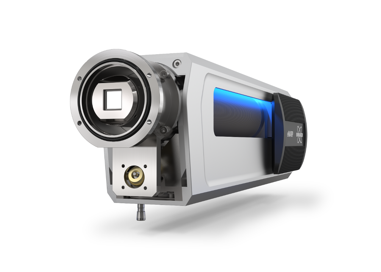
Nanostructure Characterization and Defect Identification with eWARP
This webnote discusses the nanostructural characterization of a microprocessor using our legacy EBSD detector, eFlash FS, which has now been replaced by our next-generation eWARP detector for ultra-fast, high-resolution EBSD.
eWARP's unprecedented speed advantage fully unfolds when high throughput is required for the characterization of nanostructures and potential defects, accelerating failure analysis of microelectronic devices.