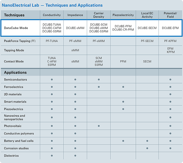
DataCube Modes
Complete Solution for Nanoelectrical Characterization
DataCube modes expand capabilities, such as PeakForce TUNA and PeakForce KPFM, by enabling the acquisition of multidimensional data cubes. For materials scientists and engineers, this breaks long-standing efficiency and characterization barriers. These new capabilities provide simultaneous capture of nanometer-scale electrical and mechanical characteristics in high-density data cubes, previously impossible to attain in a single measurement.
Correlated Multidimensional Electrical Spectroscopy
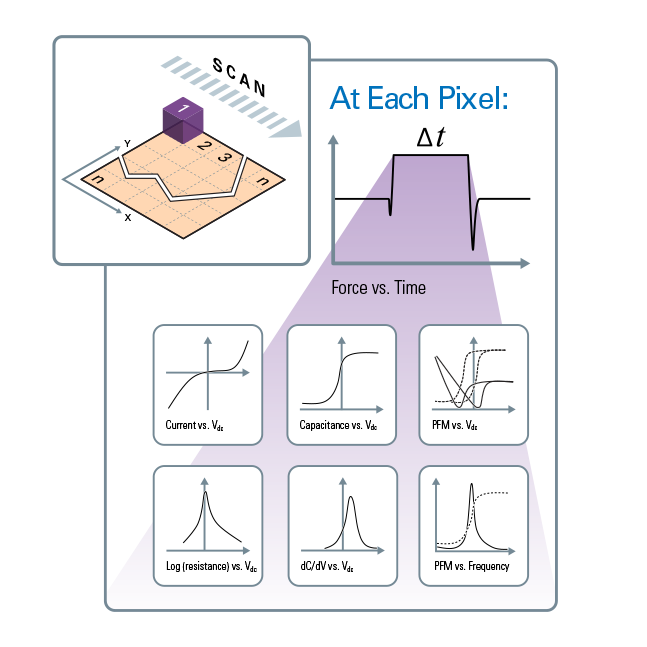
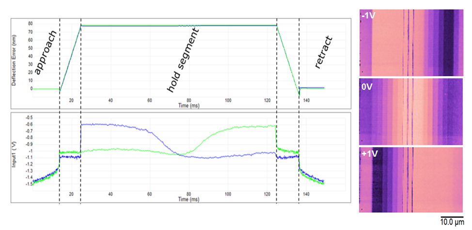
DataCube modes utilize FASTForce Volume to perform a force-distance spectrum in every pixel, with a user-defined 'dwell time'. Using high data capture rates, a multitude of electrical measurements are performed during the dwell time, resulting in electrical and mechanical spectra at every pixel. Typical force-distance spectra, measured at a ramp rate of 40 Hz with a 100 ms dwell time per pixel, provide full characterization in a single experiment, which is unheard of in a commercial AFM. It is no longer an epic experiment to simultaneously render topographical, mechanical, and multidimensional electrical information. Now such data can be achieved as a routine AFM measurement. DataCube mode renders multidimensional data cubes at nanometer-length scales with compound data in every scan. This capability enables a powerful series of new modes.
DataCube-TUNA (DCUBE-TUNA)
Conductive AFM results are influenced by the applied sample voltage, depicting important performance transitions of a material or device. DCUBE-TUNA enables simultaneous acquisition of nanomechanical information and electrical conductivity at a multitude of sample voltages in a single measurement, building a dense data cube of sample information. This is the only mode providing a complete picture of the sample conductivity, with details such as conductivity type (Ohmic, non-Ohmic, Schottky, etc.), and barrier heights.
DataCube-SCM (DCUBE-SCM)
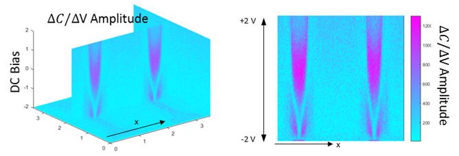
Scanning capacitance microscopy (SCM) provides a method for direct measurement of active carrier concentration with nanometer-scale accuracy. DCUBE-SCM enables simultaneous acquisition of nanomechanical and carrier information at a multitude of sample voltages in a single measurement. The technique provides a unique solution to observe dC/dV amplitude and dC/dV phase value changes and junction position shifts. Through the resulting data cubes, a researcher can observe additional information on oxide thickness, oxide charges, threshold voltages, contamination from mobile ions, and interface trap density.
DataCube-PFM (DCUBE-PFM)
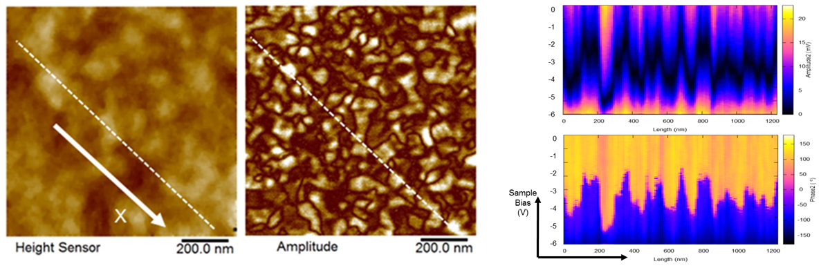
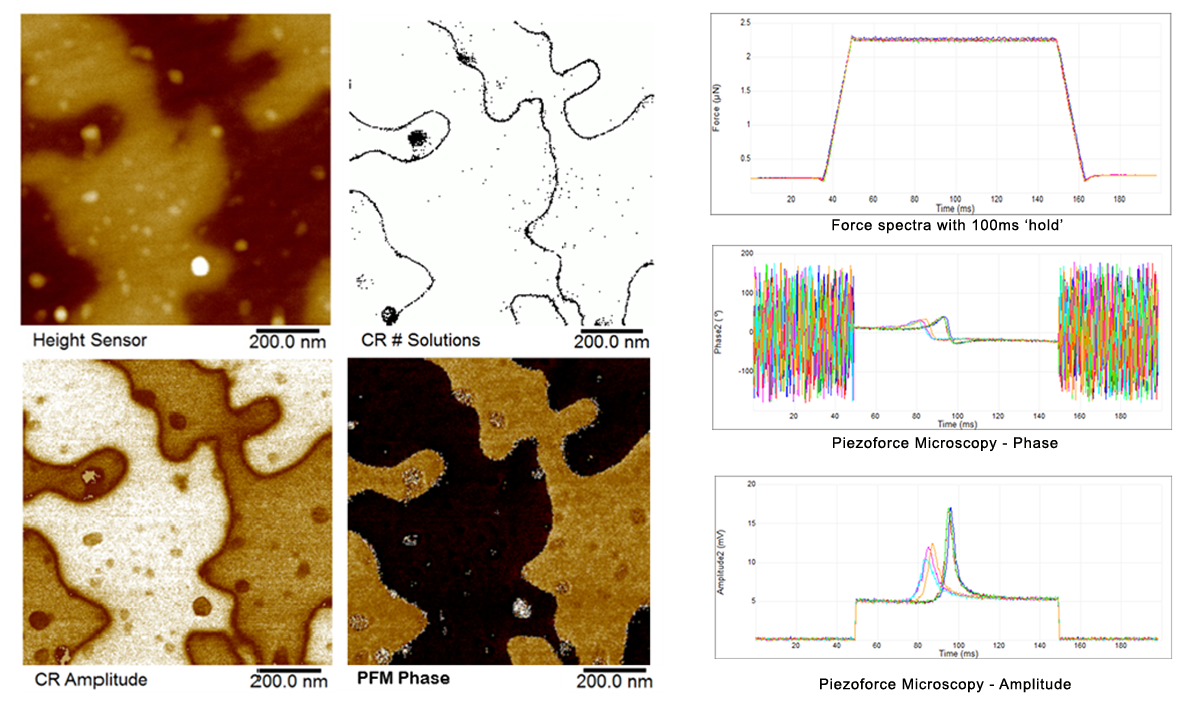
Piezoresponse (Piezoforce) Microscopy (PFM) is a technique that maps out the inverse piezoelectric effect on a sample at nanometers scale. DCUBE-PFM enables simultaneous acquisition of nanomechanical information and PFM amplitude/phase spectra in data cubes, which reveal the switching voltage of each individual domain in a single data set. In addition, DCUBE-PFM overcomes artifacts, sample damage, and complexity of data analysis associated with conventional Contact Mode approaches.
DataCube-CR-PFM (DCUBE-CR-PFM)
DCUBE piezoresponse (piezoforce) microscopy in conjunction with contact resonance provides the benefits of DCUBE-PFM with the added benefit of providing a frequency ramp at every pixel, providing a full spectrum and the peak sensitivity at the contact resonance.
DataCube-SSRM (DCUBE-SSRM)
Scanning Spreading Resistance Microscopy (SSRM) is used to map the variation in majority carrier concentration in doped semiconductors. DCUBE-SSRM enables simultaneous acquisition of nanomechanical information and 3D carrier density mapping in a single measurement. The resulting data cubes provide complete characterization including nanoscale topography, mechanical information and log-resistance spectroscopy. In addition, I-V measurements reveal conductivity whether Ohmic, non-Ohmic, Schottky, or other.
DataCube-sMIM (DCUBE-sMIM)
Scanning Microwave Microscopy Imaging (sMIM) provides maps of the capacitive (C ) and resistive (R ) part of the impedance, as well as dC/dV, and dR/dV data – at a user defined sample voltage. With DCUBE-sMIM one can acquire the same properties at a variety of sample voltages, in a single scan - and get the ‘full picture’ at once. The spectra also reveal additional information, such as conduction type (Ohmic, non-Ohmic, Schottky, etc.), oxide thickness, oxide charges, contamination from mobile ions, and interface trap density.