PeakForce sMIM
Most sensitive and complete nanoscale mapping of permittivity and conductivity
PeakForce sMIM
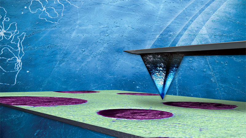
PeakForce sMIM couples sMIM with Bruker’s PeakForce Tapping® technology to greatly expand its application to previously challenging samples (e.g., carbon nanotubes, nanoparticle oxide films, and semiconductor devices) and provides simultaneous mapping of correlated nanomechanical properties.
PeakForce sMIM mode:
- Eliminates high-shear forces associated with contact-based electrical modes that can distort or dislocate delicate samples;
- Allows high-resolution imaging of rough sample surfaces and delivers highly sensitive electrical measurements by removing convolution from topographical data; and
- Enables multiparametric imaging with direct correlation to nanomechanical properties, such as modulus and adhesion.

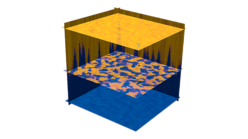
PeakForce sMIM images of carbon nanotubes (CNTs) aligned flat on an insulating substrate. The sMIM-R channel confirms these CNTs have different conductivities as indicated by the square boxes on adhesion and sMIM-R channels. (Sample courtesy Greg Michael Pitner and Professor H.–S. Philip Wong, Stanford University.)

PeakForce sMIM enables characterization of the nanoelectrical properties of fragile samples, such as carbon nanotubes (CNTs). High-resolution imaging of individual CNTs on the surface of an insulating glass substrate allows differentiation of CNTs with insulating, semiconducting, and metallic properties. The cross section (sMIM-C data channel) shows the sub-10nm resolution routinely achieved with PeakForce sMIM.