Scanning Capacitance Microscopy (SCM)
Mapping the carrier concentration across nonuniformly doped semiconductor samples has conventionally relied upon tools such as secondary ion mass spectrometry (SIMS), spreading resistance profiling (SRP), and one-dimensional capacitance-voltage (C-V). These instruments generate data in one dimension, requiring quantitative two-dimensional information to be inferred.
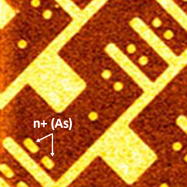
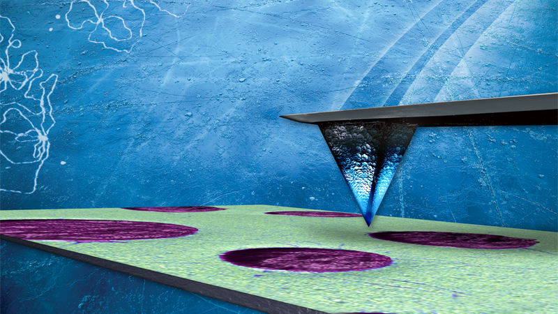
Scanning Capacitance Microscopy (SCM) provides a method for direct measurement of activated carrier concentration with nanometer scale accuracy in two dimensions. SCM is derived from Contact Mode and measures changes in capacitance between the tip and the sample surface using an extremely sensitive high-frequency resonant circuit.
In addition to SCM, Bruker offers several Nanoelectrical Characterization Modes for a wide range of electrical applications.