Scanning Spreading Resistance Microscopy (SSRM and SSRM-HR)
Light-emitting diodes (LEDs), photodetectors, and diode lasers are based on semiconductor technology, and their development and fabrication depends upon the ability to measure their electrical properties in two dimensions with high resolution.
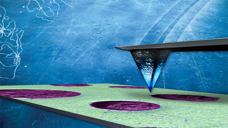
Scanning Spreading Resistance Microscopy (SSRM), like Scanning Capacitance Microscopy (SCM), enables simultaneous topographic imaging and 2D carrier density mapping on the surface of semiconductor samples. SSRM employs Contact Mode feedback at high force in conjunction with a wide range amplifier to obtain a measurement of spreading resistance and thus carrier density.
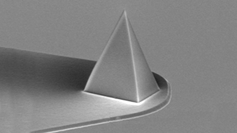
The Dimension Icon® SSRM-HR package achieves highest spatial resolution and repeatability in 2D carrier density mapping, making it the configuration of choice for leading edge semiconductor work.


Your download is now available.
Note: If you exit this page, you may not be able to reopen this download window without re-submitting the form.