
Atomic Force Microscopy Methods for Semiconductor Failure Analysis
Characterizing nanoscale topography, physical properties, and chemical composition for failure analysis
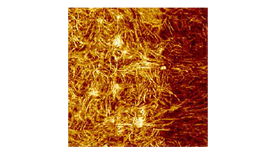
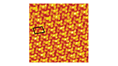
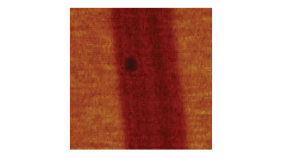
Atomic force microscopy (AFM) is well known for its standard capability to image surface topography with nanometer-scale spatial resolution. One of its greatest advantages for failure analysis is the added ability to provide complementary nanoscale information about electrical, magnetic, thermal, and mechanical properties, as well as chemical identification. This webinar focuses on the electrical, thermal, mechanical, and chemical AFM modes most important for failure analysis.
Watch this on-demand webinar to hear about AFM operating modes for failure analysis, with relevant information provided for each mode, including:
- Capabilities and limitations.
- Examples from Si-based devices and other materials.
- Practical advice for implementation.
By the end of the webinar, you will understand the AFM modes most valuable for failure analysis and be equipped to make informed decisions for your applications.
Abstract
Atomic force microscopy (AFM) and its related technologies have become essential for characterizing semiconductor materials and devices, from R&D to failure analysis and high-volume manufacturing.
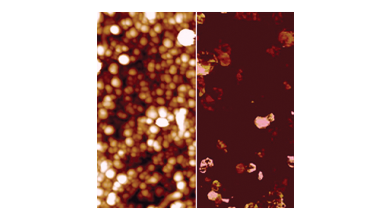
AFM's standard capability to image surface topography with nanometer-scale spatial resolution is commonly used for characterization of surface roughness, defect inspection, critical dimensions, and depth metrology with sub-nanometer precision. AFM also has the complementary ability to measure electrical, magnetic, thermal, and mechanical properties at the nanoscale. Specially equipped Bruker systems can additionally perform chemical identification at the nanoscale using patented photothermal AFM-based IR spectroscopy (AFM-IR) technology.
This webinar focuses on the electrical, thermal, mechanical, and chemical AFM modes important for failure analysis:
- Electrical modes include methods for carrying out 2D carrier profiling; mapping conductivity variations, work function, and charge related characteristics; and assessing ferroelectric, piezoelectric, or dielectric properties.
- The thermal mode of scanning thermal microscopy is used to measure local variations in temperature or thermal conductivity, even on active devices.
- Mechanical modes are used to evaluate nanomechanical properties, such as adhesion, elastic modulus, and viscoelastic modulus.
- Chemical modes can identify chemical composition of yield-killing defects and process-enabling materials, which are critical for both wafers and photomasks, especially in the EUV era.
The presenters will introduce several modes in each of these categories and highlight physical properties characterized, spatial resolution, detection sensitivity, dynamic range, and quantification potential. They will also illustrate the capabilities and limitations of each operating mode with examples from Si-based devices and other materials, such as compound semiconductors, organic devices, and 2D materials.
Presenters will also discuss practical aspects of AFM for failure analysis, such as sample preparation, probe selection and lifetime, and environmental influences.
Find out more about the technology featured in this webinar or our other solutions for Atomic Force Microscopy: