Electrical, Magnetic, and Thermal Measurements
Electric Force Microscopy (EFM)
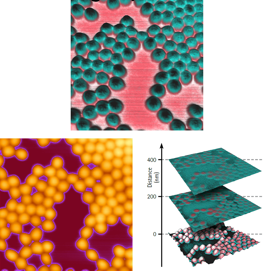
QI™-EFM on NIPAM Particles
Electrostatic force microscopy (QI™-EFM) on NIPAM particles on silicon. 3D ForceCube™ images collected with NanoWizard NanoScience, calculated at different distances between tip and sample. Scan size: 4.5 μm × 4.5 μm.
- Top: Height image (z-range: 90 nm)
- Bottom left: Overlay of electrostatic force signal (color texture range: 15 mV) and 3D topography
- Bottom right: 3D ForceCube™ images
Sample courtesy of:
Prof. R. von Klitzing
TU-Berlin, Germany.
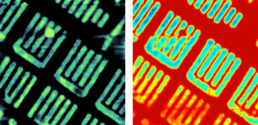
Electrostatic Force Microscopy (EFM) on SRAM
Electrostatic Force Microscopy (EFM, one-pass) on SRAM (Core I5 processor, Intel). Imaged with NanoWizard NanoScience.
- Left: Height image
- Right: Overlay of electrostatic force signal and 3D topography (scan size: 1.4 μm × 1.4 μm; color texture range: 30 mV)
Conductive Atomic Force Microscopy (CAFM)
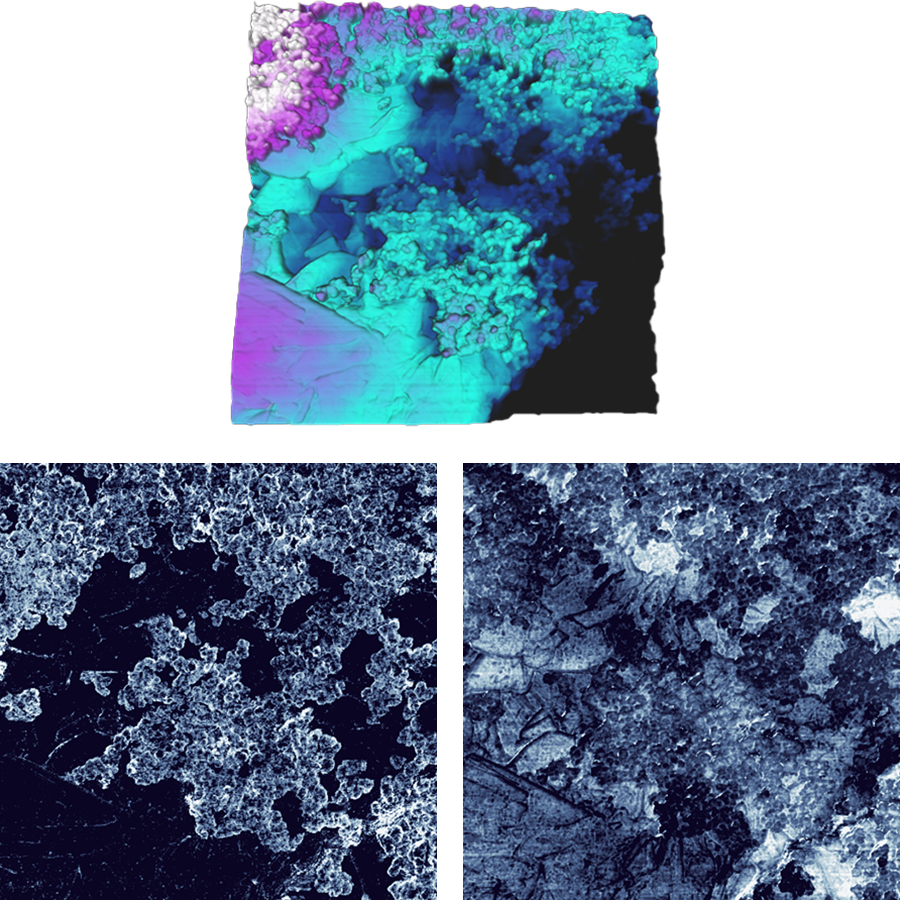
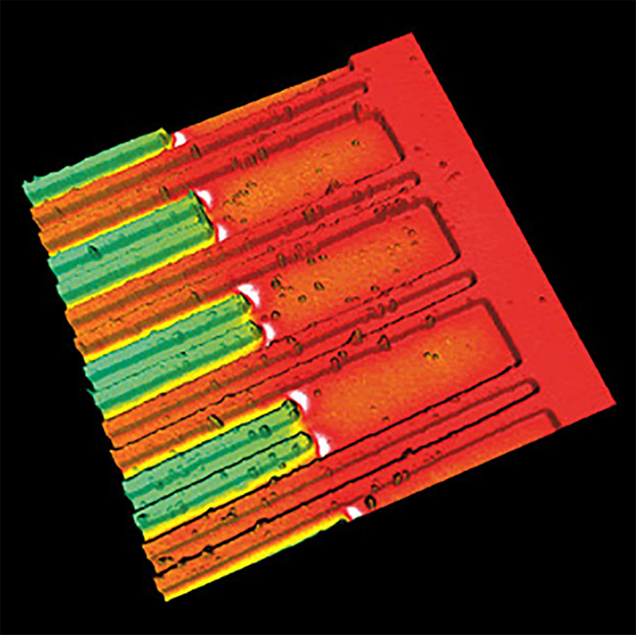
QI™-CAFM on Battery Electrode
Conductive atomic force microscopy (QI™-CAFM) on battery electrode. Scan size: 4.5 μm × 4.5 μm. Images collected with NanoWizard NanoScience.
- Top: 3D height image (z-range: 1 μm)
- Bottom Left: Adhesion image (range: 10 N/m)
- Bottom Right: Current image (range: 160 nA)
Sample courtesy of:
Prof. Dr.-Ing. A. Kwade
TU Braunschweig, Germany.
CAFM on CU Conduct Layer
Conductive atomic force microscopy (CAFM-QI™) on CU conduct layer (Core I5 processor, Intel). Scan size: 1.4 μm × 1.4 μm. Images collected with NanoWizard NanoScience.
- Left: Height image (z-range: 10 nm)
- Right: Current image (range: 15 nA)
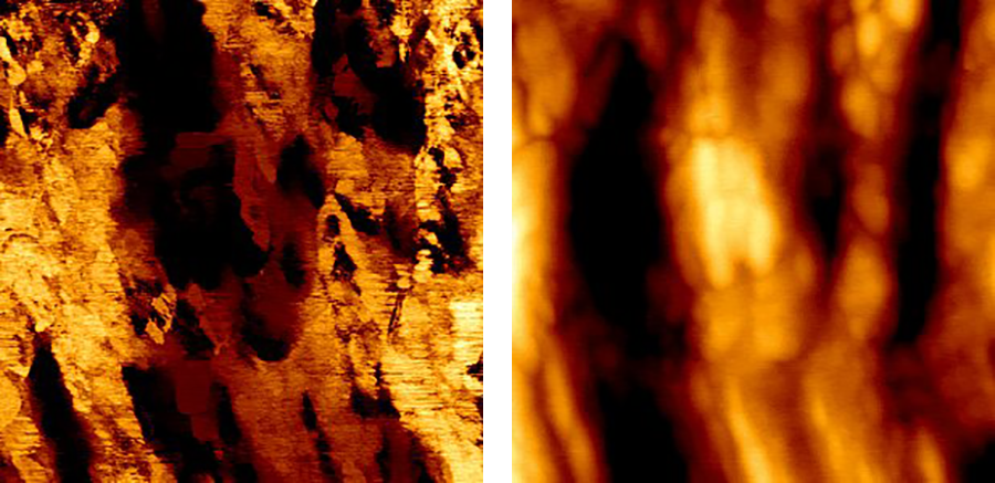
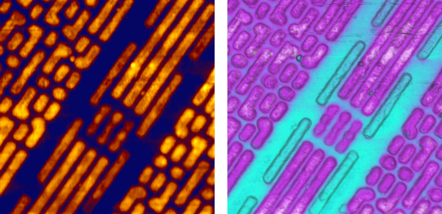
Conductive AFM of a Graphite-Clay Blend
Conductivity landscape and height image of a graphite-clay blend. Images collected with NanoWizard Sense.
- Left: CAFM image (scan field 2.5 µm x 2.5 µm; range from 0 to 20.41 nA)
- Right: Height image (scan field 2.5 µm x 2.5 µm; z-range: 36.45 nm)
Kelvin Probe Force Microscopy (KPFM)
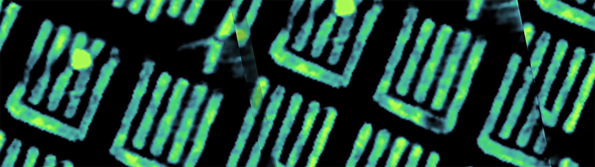
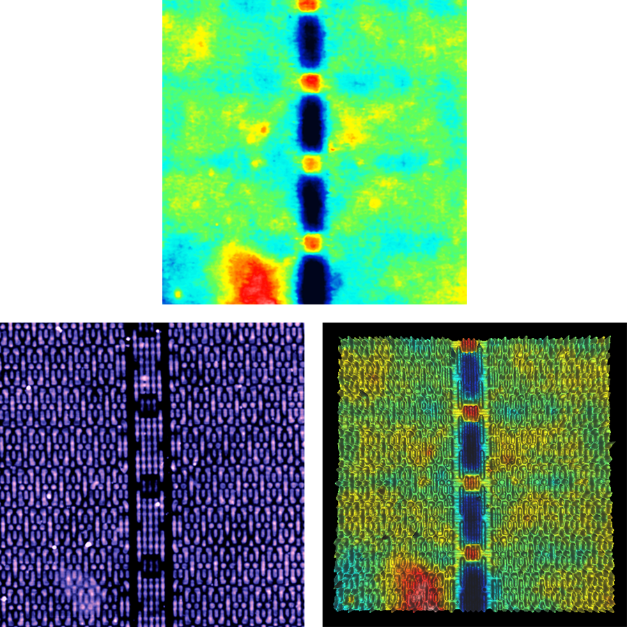
QI™-KPM on an Interdigitated Electrode
Kelvin Probe Microscopy (QI™-KPM) on an interdigitated electrode. Data collected with NanoWizard NanoScience.
3D height image is overlaid with surface potential information. The raised electrodes (100 nm thick) are interdigitated in pairs, the separation between topography and potential is clear. Scan size: 15 μm × 15 μm, color texture range: 750 mV.
KPM on an Interdigitated Electrode
Kelvin Probe Microscopy (KPM) on an interdigitated electrode. Data collected with NanoWizard NanoScience.
The height image is displayed as 3D topography with the added color to indicate measured surface potential. The raised electrodes (100nm thick) are interdigitated in pairs, the separation between topography and potential is clearly visible. Scan size: 21 µm x 21 µm.
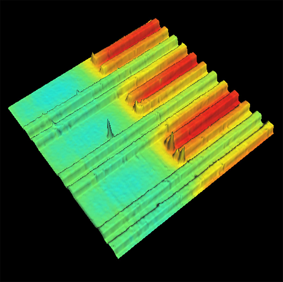
KPM on SRAM
Kevin Probe Microscopy (KPM, one-pass FM) on SRAM (Core I5 processor, Intel). Scan size: 4.5 μm × 4.5 μm. Imaged with NanoWizard NanoScience.
- Top: Surface potential (range: 50 mV)
- Bottom left: Height image (z-range: 10 nm)
- Bottom right: Overlay of 3D topography and surface potential
Magnetic Force Microscopy (MFM)
MFM on NiFe Square Structure
NanoWizard NanoScience overlay of magnetic force information and 3d height image on NiFe square structure. Magnetic domains and Landau pattern are clearly visible. Scan size 8 μm × 8 μm.
Sample courtesy of:
Dr. Katrin Schultheiss, Institute of Ion beam Physics and Materials Research
Helmholtz-Zentrum Dresden-Rossendorf, Germany
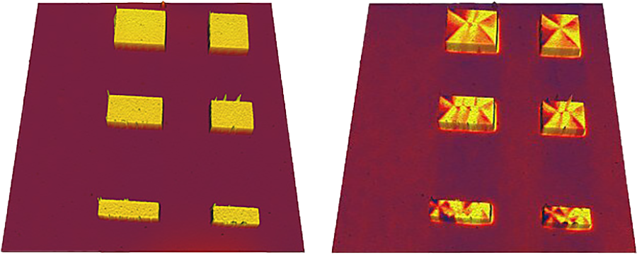
MFM Images of Six Rectangular Magnetic Structures
NanoWizard NanoScience topography and phase (MFM with magnetic cantilever) images of rectangular magnetic structures on NiFe. Magnetic domains and Landau pattern are clearly visible. Scan region 20 µm x 20 µm; z-length: 60 nm.
- Left: Height image
- Right: 3D topography image overlaid with phase information
Sample courtesy of:
Philipp Pirro
TU Kaiserslautern
MFM on Hard Drive
Magnetic Force Microscopy image (MFM) of a hard drive section. The bit structure of the hard disk (magnetic domains) can be observed. Scan size 3 µm x 3 µm. Imaged on the NanoWizard NanoScience AFM.
- Left: Height image
- Right: Magnetic force signal
Piezoresponse Force Microscopy (PFM)
Domain Visualization in Lithium Niobate Crystal (PFM)
Piezo-response phase, height, and amplitude images of lithium niobate crystal. Scan field: 21 µm x 24 µm. Images collected with NanoWizard NanoScience.
- Top left: Piezoresponse phase image
- Top right: Height image
- Bottom left: Amplitude image lateral
- Bottom right: Amplitude image vertical
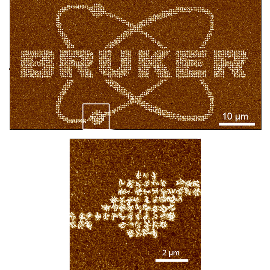
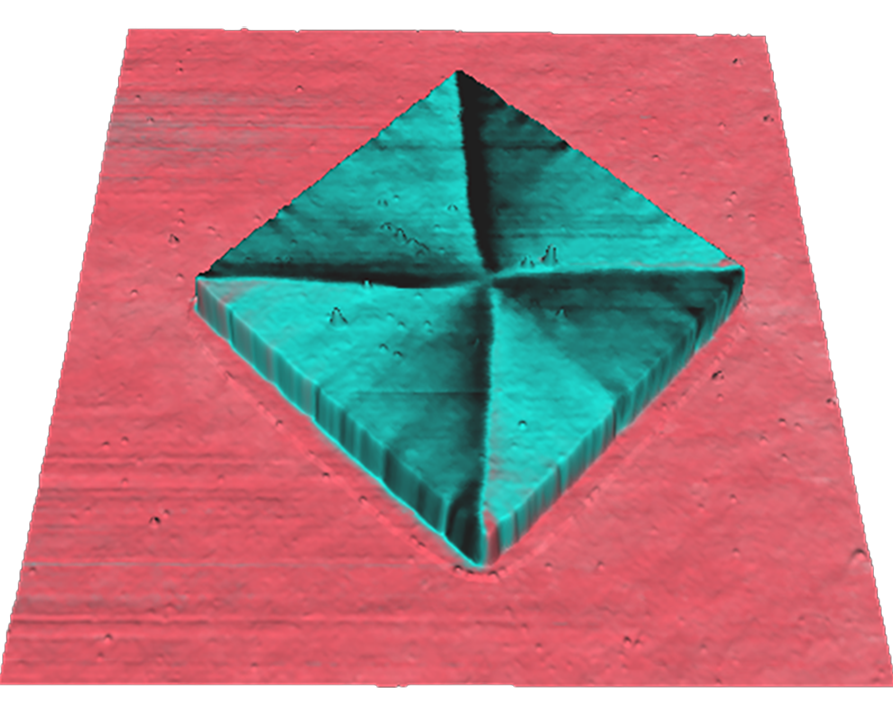
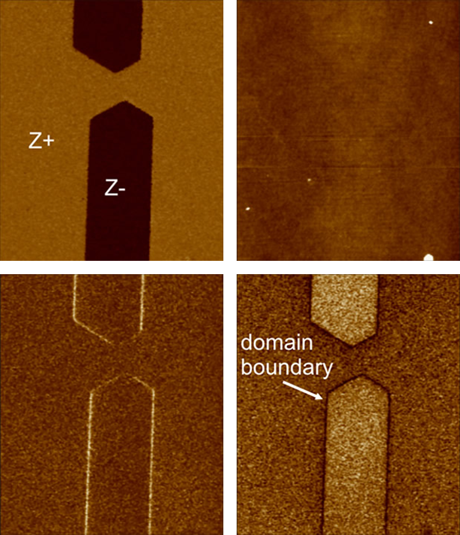
Piezoresponse Force Microscopy of a Ferroelectric Copolymer
Piezoresponse Force Microscopy (PFM) of a ferroelectric copolymer (P(VDF-TrFE)). A sequence of voltage pulses (+/-20 V range) was generated from a bitmap to write the pattern into the piezoelectric polarization of the sample. Imaged with NanoWizard Sense.
Scanning Tunneling Microscopy (STM)
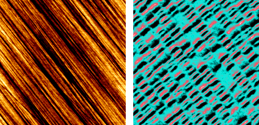
STM of Arachidic Acid Molecules
Scanning Tunneling Microscopy image (STM, current) of arachidic acid molecules on HOPG collected with NanoWizard NanoScience. Scan size: 25 nm × 25 nm; current range: 0.8 nA; bias: 0.3 V.
Scanning Thermal Microscopy (SThM)
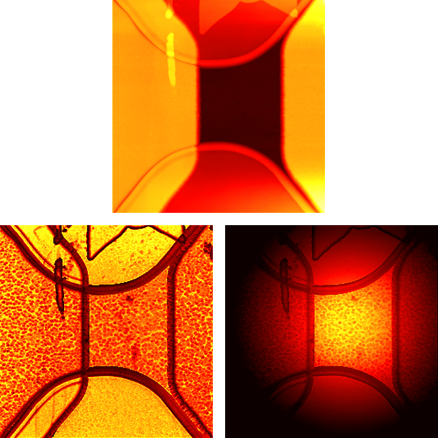
Scanning Thermal Microscopy
Scanning thermal microscopy measurement with VertiSense™ module on AppNano thermal test sample. Images collected with NanoWizard NanoScience in QI™ mode with VertiSense™ Probes. Scan size: 20 μm × 20 μm
- Top: Height image (z-range: 600 nm)
- Bottom left: Adhesion image (range: 9.5 nN)
- Bottom right: Temperature information (range: 55°C)