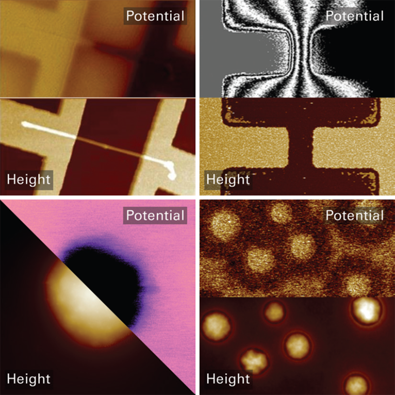
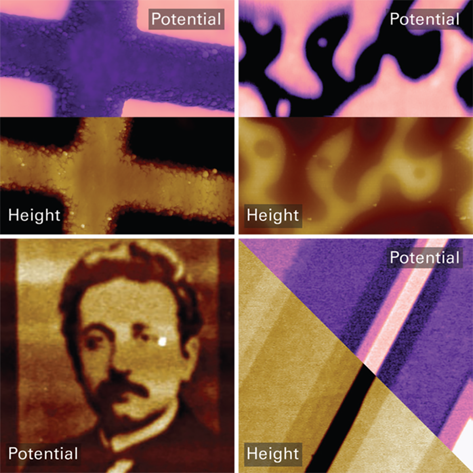
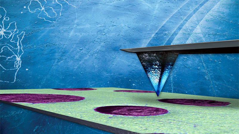
Kelvin Probe Force Microscopy (KPFM)
Metallic and semiconducting nanostructures are used in a variety of devices, from biosensors to solar cells. Researchers are interested in analyzing the surface potential of nanostructures, surfaces, and devices, as these properties strongly affect local chemical and physical phenomena. Kelvin Probe Force Microscopy (KPFM) enables high-resolution surface potential and topography mapping of a variety of samples.
Bruker offers three KPFM modes based on TappingMode™ technology:
The PeakForce KPFM™ accessory includes the above KPFM modes, as well as powerful KPFM modes based on Bruker’s patented PeakForce Tapping® technology.
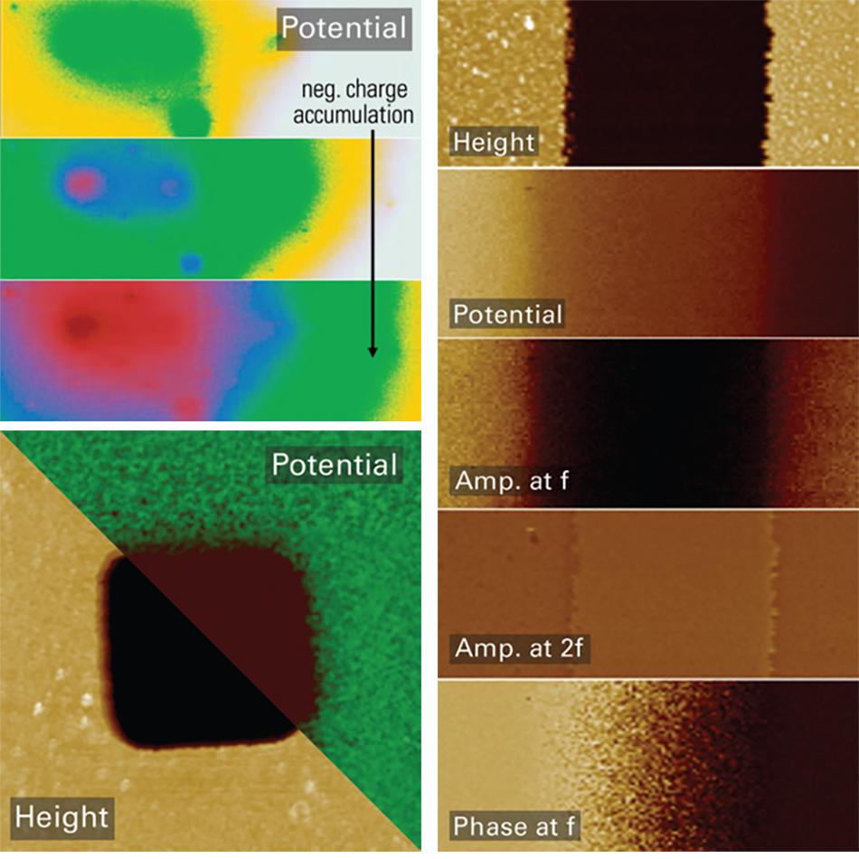
Amplitude Modulation Kelvin Probe Force Microscopy (AM-KPFM)
AM‑KPFM was the first of several KPFM methods implemented on the Bruker AFMs, and is based upon electric force detection.
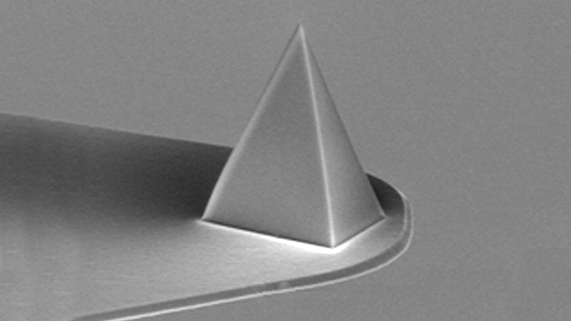
AM‑KPFM is a dual‑pass technique. In a first pass, topography is collected in TappingMode, while during the second pass (LiftMode), an AC bias is applied between the tip and sample at the resonance frequency of the AFM cantilever. The modulated electric force is measured using the oscillation of the cantilever, which is used as input to a Kelvin feedback loop where DC bias is adjusted until oscillation amplitude drops to zero. In this way, the applied voltage equals the CPD value of interest.
AM‑KPFM has found broad applications in corrosion studies of alloys, evaluation of photovoltaic effects on solar cells, and surface analysis. This mode can also be applied to map the potential distribution in active samples, such as operating semiconductor devices. AM‑KPFM is an easy‑to‑use KPFM method, but for enhanced accuracy or resolution, consider one of the other KPFM implementations: FM‑KPFM, PeakForce KPFM, or HV‑KPFM.
Frequency Modulation Kelvin Probe Force Microscopy (FM-KPFM)
FM‑KPFM is based upon electric force gradient detection and provides improved accuracy and spatial resolution over AM‑KPFM.
Unlike AM‑KPFM and PeakForce KPFM, FM‑KPFM does not use a dual‑pass technique. During the TappingMode scan, a low‑frequency AC bias is applied between the tip and sample, modulating the resonant frequency and creating sidebands. The modulated electric force gradient is measured using two cascaded lock‑in amplifiers and is used as input to a Kelvin feedback loop, adjusting a DC bias until the oscillation amplitude drops to zero. In this way, the applied voltage equals the CPD value of interest.
FM‑KPFM has found broad applications in corrosion studies of alloys, evaluation of photovoltaic effects on solar cells, mapping of trapped charges in dielectrics, and surface analysis. This mode can also be applied to map the potential distribution in active samples, such as operating semiconductor devices. FM‑KPFM provides higher accuracy, repeatability and spatial resolution than AM‑KPFM, and using a single pass also reduces image acquisition time.
High‑Voltage Kelvin Probe Force Microscopy (HV-KPFM)
HV‑KPFM belongs to the family of KPFM methods to map out surface (electrostatic) potentials. In HV‑KPFM, electrostatic potential can be measured beyond ±10 V, which is often a limit in other KFPM implementations. HV‑KPFM can be applied to a variety of samples.
KPFM‑HV is a dual‑pass technique. In a first pass, topography is collected in a PeakForce Tapping scan that also provides nanomechanical information. On the second pass (LiftMode), an AC bias is applied between the tip and sample. The vertical deflection signal is simultaneously fed to two synchronized lock‑in amplifiers (drive frequency and second harmonic). A calculation is carried out to obtain electrostatic potential difference. HV‑KFPM allows measurement of voltages in the range of ±200 V.
HV‑KPFM is of particular interest for samples where the surface potential values vary over a large range. A typical example is the measurement of trapped (immobilized) charges in insulators. As HV‑KPFM applies a so‑called open‑loop detection, it can also be of interest in experiments where avoidance of a closed‑loop Kelvin loop is desired, for example to overcome the limited response time. KPFM experiments that require a high sensitivity generally use one of the other methods, such as PeakForce KPFM.

Your download is now available.
Note: If you exit this page, you may not be able to reopen this download window without re-submitting the form.
