FilmTek 2000M
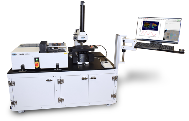
FilmTek 2000M
The FilmTek 2000M™ provides a measurement spot size as small as 1 x 2 µm and a nearly collimated beam. This approach allows accurate, non-contact measurement of thin to very thick films. With automated wafer handling, 1D/2D barcode scanner, and pattern recognition, straightforward measurements from an entire device wafer can be obtained, eliminating the need to infer broader performance from a limited sample area.
Measurement Capabilities
Enables simultaneous determination of:
- Multiple layer thicknesses
- Indices of refraction [ n(λ) ]
- Extinction (absorption) coefficients [ k(λ) ]
- Energy band gap [ Eg ]
- Critical dimension (CD) measurement
System Components
Standard:
- Spectroscopic reflection measurement
- 5nm to 350µm film thickness range
- 2µm spot size (5×10µm standard)
- Automated stage with autofocus
- Camera for imaging measurement location
- Pattern recognition
- Advanced material modeling software
- Bruker's generalized material model with advanced global optimization algorithms
Optional:
- Automated wafer handling
- SECS/GEM
Typical Application Areas

Medical Sensors & Devices
Enhance the quality, consistency, and performance of medical devices and sensors with accurate and robust thickness measurement of biologically active films.
FilmTek thin film metrology instruments enable automated non-contact measurement and whole-wafer mapping of film thickness for glucose sensors, coating thickness mapping on the surface of metal jaws, and film thickness determination for multi-layer stacks in single-use blood sensors.
Other typical application areas include:
- Wafer/CD metrology
- Compound semiconductor
- Data storage
- Flat panel display
Technical Specifications
| Film Thickness Range | 5 nm to 350 µm (5 nm to 150 µm is standard) |
|---|---|
| Film Thickness Accuracy | ±1.5 Å for NIST traceable standard oxide 1000 Å to 1 µm |
| Spectral Range | 380 nm - 1700 nm (380 nm - 1000 nm is standard) |
| Measurement Spot Size | 2 µm (5x10 µm standard with 10x objective) |
| Sample Size | 2 mm - 300 mm (150 mm is standard) |
| Spectral Resolution | 0.3 - 2 nm |
| Light Source | Regulated halogen lamp (2,000 hrs lifetime) |
| Detector Type | 2048 pixel Sony linear CCD array / 512 pixel cooled Hamamatsu InGaAs CCD array (NIR) |
| Computer | Multi-core processor with Windows™ 10 Operating System |
| Measurement Time | <1 sec per site (e.g., oxide film) |
Performance Specifications
| Film(s) | Thickness | Measured Parameters | Precision (1σ) |
|---|---|---|---|
| Oxide / Si | 500 - 1000 nm | t | 0.025 nm |
| 1 - 150 µm | t | 0.005% |