FilmTek 2000M
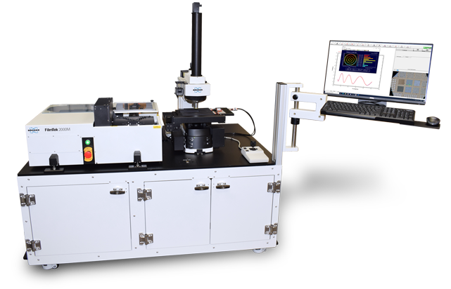
FilmTek 2000M
The FilmTek 2000M™ provides a measurement spot size as small as 1 x 2 µm and a nearly collimated beam. This approach allows accurate, non-contact measurement of thin to very thick films. With automated wafer handling, 1D/2D barcode scanner, and pattern recognition, straightforward measurements from an entire device wafer can be obtained, eliminating the need to infer broader performance from a limited sample area.
Measurement Capabilities
Enables simultaneous determination of:
- Multiple layer thicknesses
- Indices of refraction [ n(λ) ]
- Extinction (absorption) coefficients [ k(λ) ]
- Energy band gap [ Eg ]
- Critical dimension (CD) measurement
System Components
Standard:
- Spectroscopic reflection measurement
- 5nm to 350µm film thickness range
- 2µm spot size (5×10µm standard)
- Automated stage with autofocus
- Camera for imaging measurement location
- Pattern recognition
- Advanced material modeling software
- Bruker's generalized material model with advanced global optimization algorithms
Optional:
- Automated wafer handling
- SECS/GEM
Typical Application Areas

Medical Sensors & Devices
Enhance the quality, consistency, and performance of medical devices and sensors with accurate and robust thickness measurement of biologically active films.
FilmTek thin film metrology instruments enable automated non-contact measurement and whole-wafer mapping of film thickness for glucose sensors, coating thickness mapping on the surface of metal jaws, and film thickness determination for multi-layer stacks in single-use blood sensors.
Other typical application areas include:
- Wafer/CD metrology
- Compound semiconductor
- Data storage
- Flat panel display
Technical Specifications
| Film Thickness Range | 5 nm to 350 µm (5 nm to 150 µm is standard) |
|---|---|
| Film Thickness Accuracy | ±1.5 Å for NIST traceable standard oxide 1000 Å to 1 µm |
| Spectral Range | 380 nm - 1700 nm (380 nm - 1000 nm is standard) |
| Measurement Spot Size | 2 µm (5x10 µm standard with 10x objective) |
| Sample Size | 2 mm - 300 mm (150 mm is standard) |
| Spectral Resolution | 0.3 - 2 nm |
| Light Source | Regulated halogen lamp (2,000 hrs lifetime) |
| Detector Type | 2048 pixel Sony linear CCD array / 512 pixel cooled Hamamatsu InGaAs CCD array (NIR) |
| Computer | Multi-core processor with Windows™ 10 Operating System |
| Measurement Time | <1 sec per site (e.g., oxide film) |
Performance Specifications
| Film(s) | Thickness | Measured Parameters | Precision (1σ) |
|---|---|---|---|
| Oxide / Si | 500 - 1000 nm | t | 0.025 nm |
| 1 - 150 µm | t | 0.005% |
How Can We Help?

Bruker partners with our customers to solve real-world application issues. We develop next-generation technologies and help customers select the right system and accessories. This partnership continues through training and extended service, long after the tools are sold.
Our highly trained team of support engineers, application scientists and subject-matter experts are wholly dedicated to maximizing your productivity with system service and upgrades, as well as application support and training.