Application Note: Scratch Testing of Nanofilms for Flexible Electronics
Critical-Load Scratch Testing for Flexible Electronics R&D and QC
Metallic nanofilms on polymer substrates are used for a variety of applications in flexible electronics. To ensure the reliability of such flexible electronic devices, the scratch adhesion property of the nanofilm is evaluated for critical normal load as a part of R&D and QC activities. However, the evaluation of nanofilms for their adhesion properties is quite challenging.
This application note discusses the capabilities of Bruker's scratch test system and provides an example of its evaluation of a metallic nanofilm on a polymer substrate. Progressive-load scratch testing was performed with a tungsten carbide ball, and automated optical imaging and 3D profiling characterized the failure.
Readers can expect to find:
- A description of the UMT TriboLab-based Universal Scratch Test system and its force sensor and tip options
- Progressive-load scratch test results on a metallic nanofilm over a polymer substrate
- A statistical summary of critical-load values from 10 repeated scratch tests
KEYWORDS: Tribometer; Mechanical Tester; AN1012; Bruker; Technical Note; UMT TriboLab; Universal Scratch Test; Nanofilm; Flexible Electronics; Critical Load

Introduction
Metallic nanofilms on polymer substrates are widely used as interconnect components for flexible electronic devices, such as paper-like electronic display, wearables, electronic skin, solar cells, identification tags, and antennae structures.1,2 This is due to their inherent advantages of mechanical flexibility, low specific weight, low cost, and ease of integration, as compared to silicon-based counterparts. The polymer substrate mostly bears the service loads and the metallic film maintains its function without rupturing until a fairly large amount of strain is applied. The metallic nanofilm exhibits superior mechanical and electrical properties, particularly in fracture toughness, yield strength, and electrical conductivity under the action of cyclic straining. Nevertheless, the adhesion property of a nanofilm to its substrate is extremely important to avoid performance issues in overall durability and reliability of the flexible device. A poor adhesion property can cause a premature failure of the film and make the flexible electronic components useless. The two most common failure modes of such nanofilms are fractures and interface delamination.
Scratch testing is a reliable and relatively fast method that can be adopted easily for inline quality control of films during production.3-5 However, it is always challenging to perform scratch tests on such thin and flexible films. The use of a nanomechanical tester for such evaluation is limited by the force range to initiate failure of the film during scratch, as their sharp tips can cut through the film without cracking and delaminating. Nanomechanical tools also have limited productivity as the test preparation is inherently time-consuming. On the other hand, Bruker’s Universal Scratch Test system is designed specifically to address this issue and perform easier, faster, and more reliable critical load scratch failure evaluations of nanofilms.
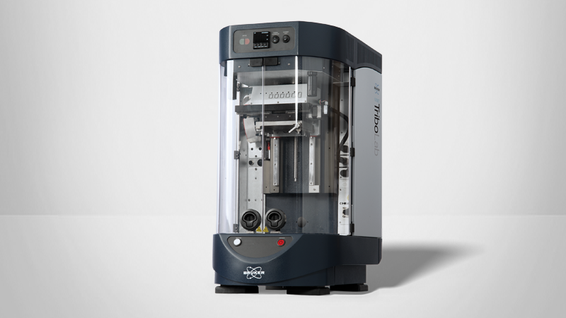
The UMT TriboLab Scratch Test System
Bruker’s scratch test system is built on the UMT TriboLab™ platform, which provides precision control of load, speed, and position. The system’s modular design ensures the flexibility to scratch test over a wide range of forces and velocities. TriboLab utilizes three major drive systems, carriage, slider, and Y-stage for Z-, X-, and Y-motion, respectively. Integrated “intelligent” hardware (TriboID™) and software (TriboScript™) interfaces make the tester an extremely user-friendly, versatile, and highly productive scratch tool. The TriboID feature not only automatically detects the various components attached to the system, but it also configures them. TriboScript offers an enhanced and secured scripting interface for easy compilation of scratch test sequences from the built-in test blocks. The system is also equipped with real-time control and data analysis software to ensure high accuracy and repeatability.
Bruker’s scratch test system can be used successfully for all modes of scratch testing, including progressive and constant load conditions. The carriage drive provides the motion along Z-direction for loading and displacement. The carriage also accommodates the slider drive that houses a force sensor and an optical microscope. The slider provides motion along the X-direction. The linear stage is used for mounting the test specimen and providing movement along the Y-direction. The scratch test system has options for the simultaneous measurement of electrical contact resistance (ECR), electrical surface resistance (ESR), acoustic emission (AE), and in-situ scratch depth profiling using a capacitance sensor for tip-displacement measurement, and optical microcopy for automated imaging of the entire scratch. Bruker’s data viewer software allows for plotting of the image of the entire scratch along with other data, such as lateral force (Fx), normal force (Fz), AE, scratch distance, scratch depth, ECR, and ESR.
Several force sensors [FVL: 1 to 100mN; FL: 5 to 500mN; DFM series: 0.05 to 20N; DFH series: 0.5 to 200N] and scratching styli/tips [diamond stylus: 2.5, 5, and 12.5μm tip radius; Rockwell indenter: 200μm tip radius with 120° cone angle; Vickers indenter (4-sided pyramid with a 136° apex angle), Knoop indenter with two apex angles (130° and 172°50/); microblade (tungsten carbide, diamond)] are available.
Test Method
The scratch test of the metallic nanofilm on a polymer substrate was performed with a tungsten carbide ball (1.6mm diameter) and a DFH-1 force sensor. The film specimen was mounted on the Y-stage and the ball was installed under the force sensor. The scratch test was performed by applying an initial load of 0.2N on the film with the ball, followed by moving the specimen over a distance of 2mm at a velocity of 0.02mm/s. During the movement of the test specimen, the normal load (Fz) was linearly increased from 0.2 to 8N. Fx and Fz data were recorded during the test. After the test, the imaging of the entire scratch was performed automatically. The scratch was further evaluated using a Bruker 3D optical microscope for the dimensions and profile of the scratch at several locations.

Results
Figure 1 shows the plots of lateral and normal forces during a progressive load scratch test of the metallic nanofilm on a polymer substrate. A gradual increase in the lateral force was observed. Figure 1 also depicts the optical image of the entire scratch (top). The width of the scratch at the end was about 238μm, as evidenced from the Δx value of the image ruler at the right-top corner in Figure 1. It is confirmed that the film started failing at a normal load of 3.42N, as indicated in Figure 1 with a vertical dashed line that corresponds to the initiation of the semi-circular cracks on the film. The corresponding Fx value was 0.66N. Unlike the scratch test of thick film, there was no sharp discontinuity in the Fx plot at the start of the failure of the nanofilm. Perhaps the lateral force was mostly dominated by the plastic deformation of the specimen at such a high normal load and not necessarily due only to the resistance of the nanofilm to fail. The semi-circular cracks at the starting of the failure were likely formed at the trailing surface of the tungsten carbide sphere where the film was subjected to a tensile load. Such failure could also be due to strain localization, such as necking after debonding of the nanofilm from the polymer substrate, as suggested by others.1 Since the film was ductile in nature, no other brittle failure mode was observed under the present test conditions. The size of the semicircular crack increased with further increase of the normal load. At about 6.7N of Fz, the film shows a large crack that was possibly formed by a secondary crack that connected the two adjacent semicircular cracks. At such a high tensile stress, the substrate started failing too.


The scratch surface was further analyzed using a Bruker 3D optical microscope (interferometer) to learn more about the dimension of the cracks thus formed. Figure 2 presents a surface profile of the semicircular cracks that formed at the critical value of Fz. It shows three such cracks. The first crack has a projected length of 80μm. The depth profile along the YY-line in Figure 2 is presented in Figure 3.
It should be noted that the scratch direction was from the bottom to the top in Figure 2. The depth profile in Figure 3 shows that at the point of the scratch there was an overall change in height of about 300nm. The rear edge of the first crack was almost 200nm above the surface and the leading edge was about 100nm below the surface. This could be due to the spallation of the nanofilm at the rear edge before the complete failure of the film under tension, thereby elevating the edge. On the other hand, the leading edge was pressed down because the sphere was still in contact, thereby likely causing such a discontinuity in the scratch profile. The scratch depth below the surface was similar to the thickness range of the nanofilm. One of the large failed areas was also examined using the interferometer. The surface profile near the large failed area is presented in Figure 4. The depth profile along the YY-line in Figure 4 is depicted in Figure 5. The failed area has a depth of 2μm. Unlike the profile in Figure 2, Figure 5 does not exhibit any rise in the profile at the rear edge, possibly because the nanofilm failed due to excessive deformation of the substrate at a higher stress level.
The scratch test was repeated 10 times to provide statistical data on the critical value of Fz for the start of failure. The values of the critical normal load for failure are presented in Table 1 for all the tests. The average value of the critical load was 3.39N, with a standard deviation (SD) of 0.26N. The scratch data thus presented confirmed that Bruker’s scratch test system can successfully perform scratch testing on metallic nanofilms on a polymer substrate for flexible electronic applications.

Conclusion
Though quite challenging, scratch testing to evaluate the adhesion property of metallic nanofilms as the critical normal load for failure in scratch is very important for the R&D and QC of flexible electronic devices. Bruker’s universal scratch test system, based on the UMT TriboLab, is capable of accurately evaluating such metallic nanofilms. The availability of sensors with wide force ranges, advanced scratch tips, and easy-to-use automated optical imaging sets this scratch test system apart from the other such instruments and methods
References
- Li, T., Huang, Z. Y., Xi, Z. C., Lacour, S. P., Wagner, S., Suo, Z., Delocalizing strain in a thin film on a polymer substrate, Mechanics of Materials, Vol. 37 (2005) 261-273.
- Lu, N., Suo, Z., Vlassak, J. J., The effect of film thickness on the failure strain of polymer-supported metal films, Acta Materialia, Vol. 58 (2010) 1679-1687.
- ASTM C1624-05 (2015), Standard Test Method for Adhesion Strength and Mechanical Failure Modes of Ceramic Coatings by Quantitative Single Point Scratch Testing, ASTM International, West Conshohocken, PA, 2015, www.astm.org
- Bull, S. J., Failure mode maps in the thin film scratch adhesion test, Tribology International, Vol.30 (1997) 491-498.
- Blees, M. H., Winkelman G. B., Balkenende A. R., den Toonder, J. M. J., The effect of friction on scratch adhesion testing: application to a sol–gel coating on polypropylene, Thin Solid Films, Vol. 359 (2000) 1-13.
Author
- Suresh Kuiry, Ph.D., Senior Applications Scientist,
Bruker Nano Surfaces Division (suresh.kuiry@bruker.com)