
Defects & Contamination
Bruker provides a range of X-ray products for determining crystalline defects and metal contamination.
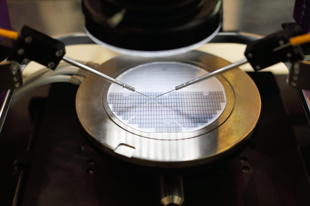
Defects & Contamination
Bruker (and previously bede and Jordan Valley) were pioneers of digital X-ray Diffraction Imaging (XRDI) in the semiconductor industry to identify killer defects causing wafer breakage, and this has expanded into identifying defects in other substrates which can affect the yield of substrates and devices. Bruker also provides TXRF systems for Si and SiC substrates for the identification of metal contamination on substrates, critical for the production line yield. For off-line inspection, Bruker offers SEM and TEM based solutions including Energy Dispersive X-ray Spectroscopy (EDS), Wavelength Dispersive X-ray Spectroscopy (WDS) and Electron Backscattered Diffraction (EBSD).