Advanced Application Examples using SEM-EDS
Element Analysis with Energy-Dispersive Spectrometry
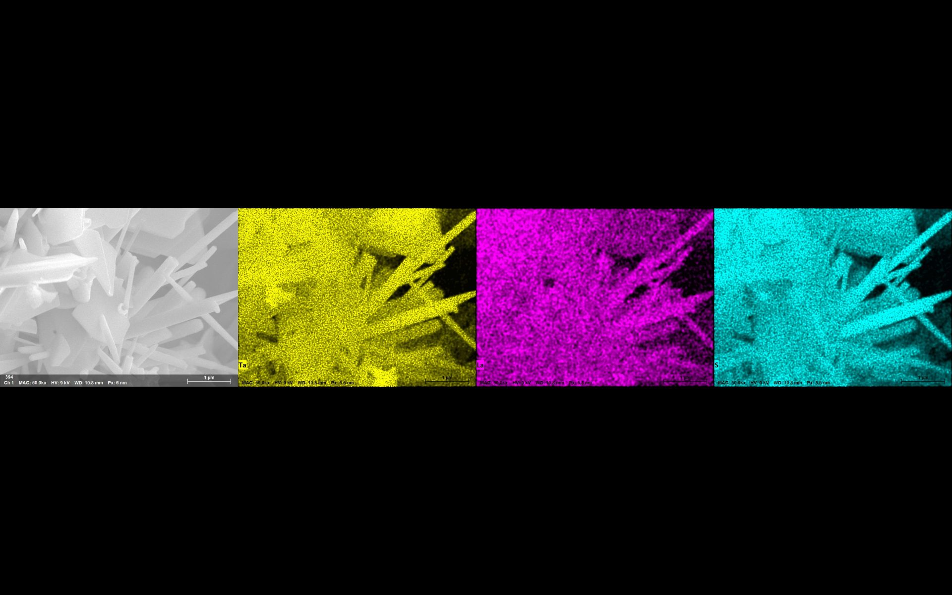
Measuring beam sensitive samples, samples with topography, or nanomaterials, can be very challenging using SEM-EDS. To investigate such samples, low voltages must be used to avoid beam damage or charging effects. This also keeps the interaction volume of the electron beam small. However, using a low voltage and low beam current has the disadvantage that not all element lines can be excited and that the count rate is not sufficient for a timely analysis.
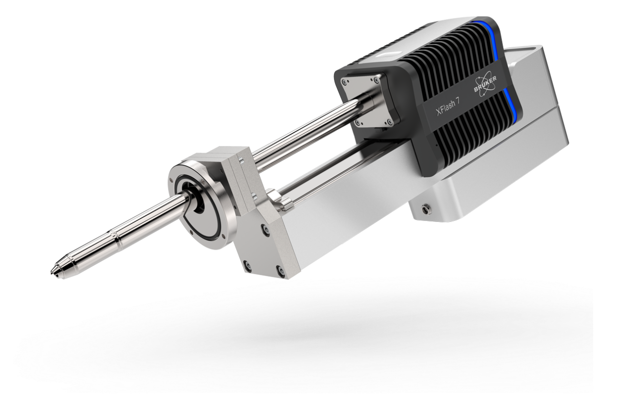
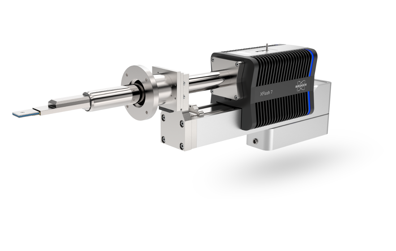
The XFlash® FlatQUAD detector with an annular design has been developed to overcome the limitations for standard EDS analysis. The XFlash® FlatQUAD has four separate multiple element SDDs integrated onto one chip, but with separate electronics. The large active area and the annular geometry, where the detector elements are very close to the X-ray source, lead to an extremely large solid angle of more than 1 sr. Therefore, extremely high-count rates can be achieved easily, even with low probe currents. These properties make the detector an ideal device for the aforementioned sample types. In addition, a better spatial resolution can be achieved as lower voltages can be used in SEM for collecting the X-ray signal.
Results from nanoscale materials acquired with the QUANTAX FlatQUAD system as well as life science applications acquired with a standard silicon drift detector will be shown in this webinar from Bruker with guest speaker from the Electron microscopy Unit at the Weizmann Institute of Science.


Who should attend?
- Scientist from all analytical fields interested in EDS technology for SEM
- Researchers working with topographically complex, three-dimensional and beam sensitive samples
Speakers

Dr. Ifat Kaplan-Ashiri
Associate Staff Scientist, Weizmann Institute of Science

Max Patzschke
Application Scientist EDS, Bruker Nano Analytics
Watch this Webinar On-Demand
Please enter your details below to gain on-demand access to this webinar.