X-Ray Metrology Systems
Non-Destructive X-ray Technology for Films and Wafers
Bruker provides advanced, non-destructive X-ray metrology solutions for characterization, process monitoring, and analysis across silicon and compound semiconductor manufacturing environments.
Our X-ray metrology portfolio supports everything from QC monitoring of epilayer films and high-throughput production metrology to detailed R&D analysis of semiconductor films, wafers, and advanced device structures. Covering the full range of processing in both logic and memory, these solutions support front-end-of-line control of epi films and high-k dielectrics, identification of substrate defects, analysis of metal films and wafer-level packaging bumps, and characterization of complex semiconductor materials and epilayer structures. Specialized systems are available for both high-volume manufacturing environments and multi-application research workflows supporting current and future metrology needs.
These solutions help semiconductor manufacturers gain the high-quality process monitoring, precision characterization, and process insight needed to accelerate development and improve manufacturing control.
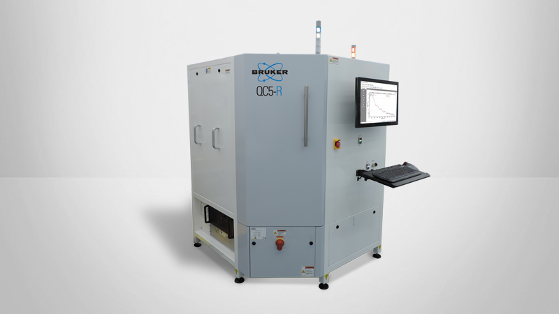
Find the Best Autmated X-Ray Metrology Solution for You
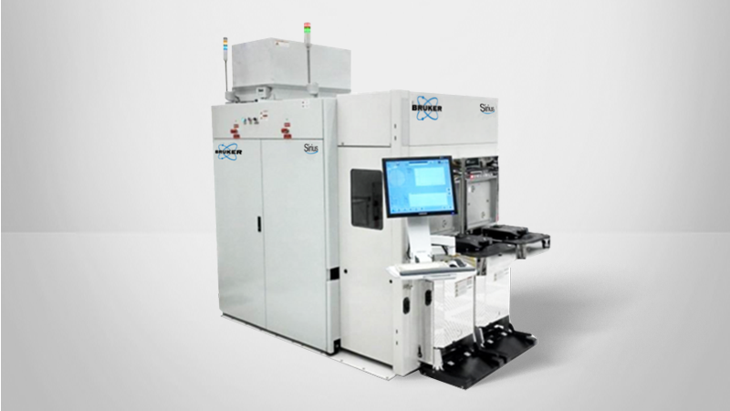
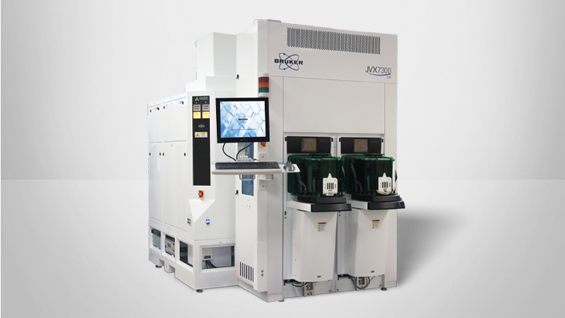
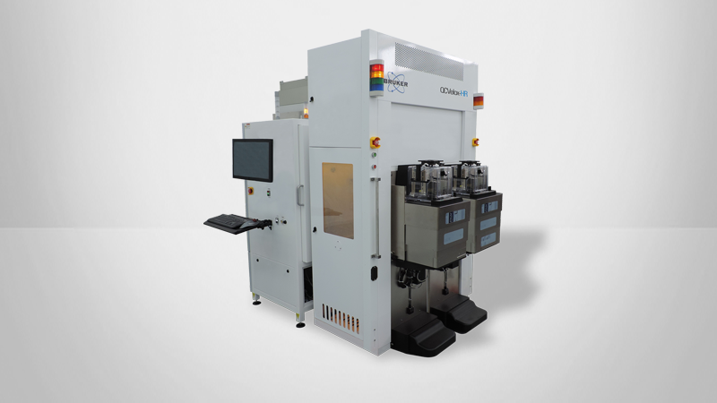
X-Ray Metrology Systems for Silicon Semiconductor

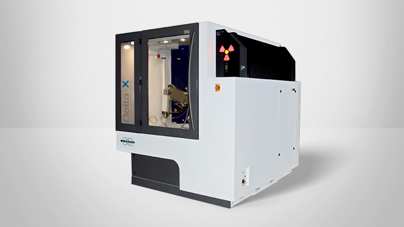
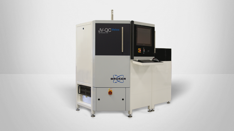
X-Ray Metrology Systems for Compound Semiconductor
X-Ray Metrology Solutions for Semiconductor Manufacturing Applications
Bruker's automated X-ray metrology solutions provide high-quality process monitoring and non-destructive characterization for silicon and compound semiconductor manufacturing, supporting everything from front-end process control and epitaxial film analysis to packaging metrology, defect identification, and detailed R&D investigations.
To learn more, contact us to discuss your measurement requirements, find out about the systems best-suited for your application, discuss options for system specialization, or request a quote based on your specific needs.

Epitaxial Film & Thin Film Characterization
Support QC monitoring of epilayer films and detailed characterization of semiconductor films, wafers, and advanced material structures for both production and research environments.
- Nanosheet thickness and composition metrology
- Thin film crystalline measurements
- QC monitoring of epilayer films
- Detailed R&D analysis of semiconductor films and wafers

Front-End Process Control & Advanced Device Metrology
Provide front-end-of-line process control of epi films and high-k dielectrics across logic, memory, and power semiconductor manufacturing.
- Advanced memory high-aspect ratio 3D metrology
- Power devices FEOL process monitoring

Packaging & Metallization Analysis
Analyze metal films, wafer-level packaging structures, and metallization processes used in advanced semiconductor devices.
- Bump metallization process monitoring
- BEOL metallization process monitoring

Defect Inspection & Process Monitoring
Enable high-quality process monitoring and identification of substrate defects across development, process optimization, and high-volume manufacturing environments.
- Identification of substrate defects
Get Expert Answers
Ask us a question, request more information, or get in touch with a Bruker sales representative.