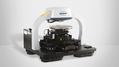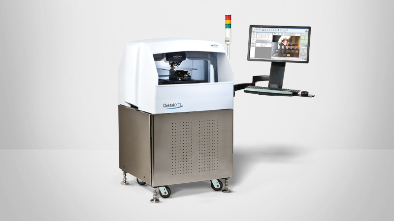

Accurate Metrology for Micro- and Nano-Fabrication with Stylus Profilometry
Learn About the Applications and Best-Practices of Stylus Profilometry
This presentation includes:
- An overview of the main components and measurement capabilities of stylus profilometers.
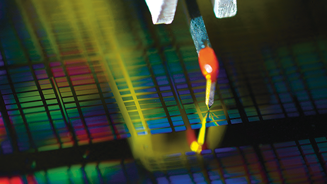
- A review of how stylus size and shape impact data acquisition, as well as when to use different types of stylus probes.
- Real-time demonstrations of several measurements for process verification, including using a stylus profilometer to measure step height, surface roughness, and wafer bow/film stress.
This workshop was recorded on: March 17, 2021
Program Notes
Many processes during micro/nano-fabrication require accurate and repeatable validation of surface profiles to ensure optimum product. In this workshop, we discuss aspects critical to achieving reliable and repeatable metrology using contact-type or stylus-type profilometers. You’ll see, through real-time demonstration, several common and important measurements for process verification.
Specifically, we address how to:
- Accurately measure repetitive features for their height/depth, width, and pitch with ‘Trace Analysis’ software;
- Confidently use a stylus profilometer to measure surface roughness by selecting a stylus based on international standards and quantifying different roughness and waviness parameters;
- Automate critical measurements and data analysis;
- Obtain accurate measurements on hard and soft films by selecting the right stylus size and force;
- Determine the nature and magnitude of film-induced stress across an entire wafer; and
- Measure small surface details with 3D areal mapping and sharp stylus probe.
Additionally, we review best-practices for successful, repeatable step height and film thickness measurement using a stylus profilometer, as well as the functionalities that are fundamental to achieving the best results (including tilt correction, substrate form removal, step detection, etc.). We also highlight some features and functionalities that make Dektak an excellent tool for validating lithography, thin film deposition, etching, and micromachining steps where there is a need to measure small step heights.