Edge Roll-Off Metrology
From Perimeter to Precision: Edge Metrology That Sees What Others Miss
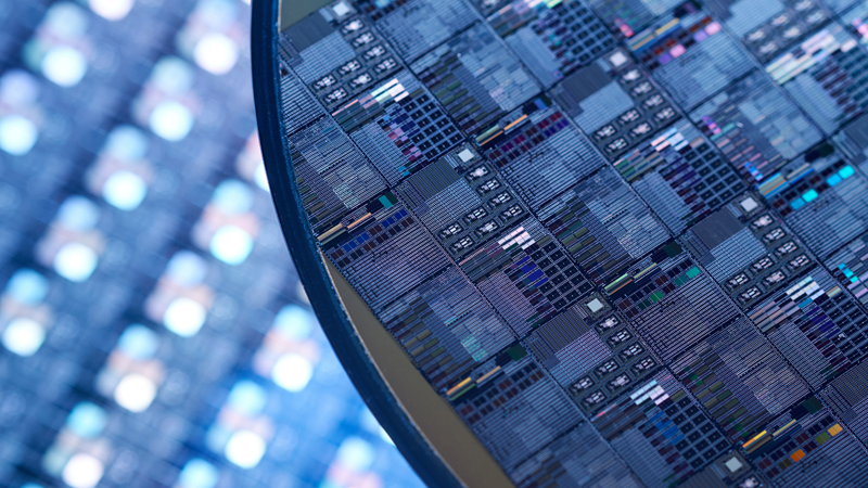
Advanced edge metrology detects edge roll-off, edge trim depth, roughness, microcracks, delamination, epi-crowing and bonding non-uniformities. It helps increase edge yield via early detection of wafer edge defects and enables advanced packaging involving wafer-to-wafer hybrid bonding.
As the semiconductor industry pushes the boundaries of scaling, packaging, and integration, the wafer edge has increasingly become a focus in efforts to improve wafer yield. Precision edge roll-off measurements offer manufacturers the ability to better monitor and control device reliability and performance — preventing failures before they start.
What is Edge Roll-Off Metrology?
Edge roll-off (ERO) — the gradual thinning or height loss near the edge caused by processes such as grinding, chemical mechanical planarization (CMP), coating, and edge trimming — is a central concern in semiconductor manufacturing.
Once overlooked, the wafer edge is now recognized as a yield-limiting region that is impacted by:
- Process non-uniformity
- Mechanical stress and chipping
- Patterning and alignment challenges at the edge
Edge roll-off metrology focuses on the high-precision measurements of wafer topography, thickness variation, roughness, and structural integrity at the wafer perimeter. By capturing ERO, crown/dish profiles, micro-cracks, and structural anomalies, edge metrology enables fabs to:
- Prevent wafer breakage and edge chipping
- Recover high value dies near the perimeter
- Improve bond quality and interconnect reliability
- Support advanced packaging flows and emerging power delivery trends
Application areas: Where Edge Metrology Delivers Impact
Hybrid Bonding: Edge Trim and ERO monitoring
- Hybrid bonding in advanced packaging means tighter overlay and thinner wafers.
- Wafer thinning increases edge fragility, making early ERO detection critical for bonding yield and mechanical stability.
- Edge roll-off monitoring prevents die yield loss.

Backside Power Delivery Networks (BSPDN): Advanced Logic Nodes
- BSPDN enables controlled wafer thinning, TSV Reveal, and edge co-planarity for bonding.
FEOL Process Control: Epitaxial Crowning, Edge Bead Removal (EBR)
- Localized edge thickening from epitaxy requires removal to ensure flatness and avoid bonding defects.
- CVD process tools suffer from an epitaxial crowning process issue, which creates uneven bonding zones along the edges.


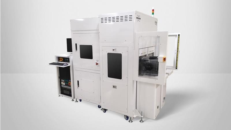
What Sets Bruker's Edge Metrology Apart
Purpose-built accuracy at the edge
- Our systems are designed to operate precisely where traditional metrology fails — the wafer perimeter.
- Orthogonal stitch scanning delivers true edge roll-off profiles, not interpolated approximations.
Automation that scales with fab throughput
- Site generation, alignment, and data output are fully automated — no manual steps.
- Seamless integration into fab workflows, with SPC-compatible outputs, minimizes setup and increases throughput.
Robust pattern recognition, not just center alignment
- Multi-point recognition aligns accurately with edge structures, enabling consistent repeatability even with edge deformation or partial patterning.
Data you can act on
- Exportable .csv and annotated image formats make it easy to feed insights into your Statistical Process Control (SPC), or yield analysis tools — no custom parsing needed.
Nanoscale precision and repeatable results
- Bruker systems are engineered for highly repeatable measurements at nanoscale precision with robust edge profile measurements.
Advanced edge characterization
- Fully automated edge profiling with zone-based segmentation extracts key ERO parameters — including slope, roughness, average step height, and transition gradients — enabling comprehensive wafer edge behavior analysis.
Trusted by leading semiconductor manufacturers
- Our solution is validated in production for CMP wafer thinning, edge trim and backgrinding — where edge process control directly impacts die yield and reliability.