Nanosheet Development
Nanosheet Development
Future nodes will implement nanosheet technology. In this technology it is a challenge to measure and control the individual thickness and composition of multiple epitaxial layers.
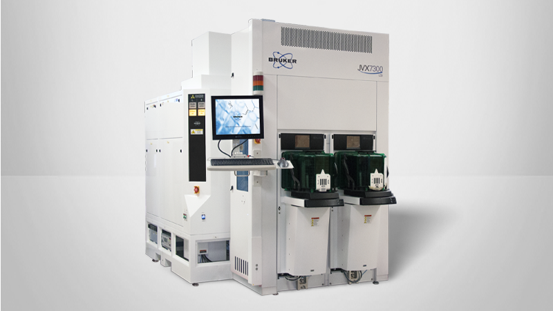
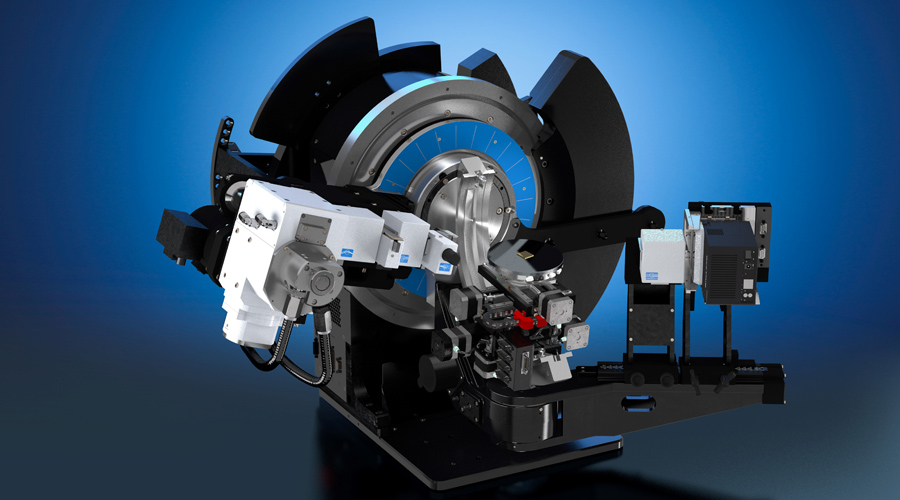
These Measurements Are Routine on our JVX7300LSI System
The stack is comprised of multiple Si and SiGe layers. Existing HVM metrology cannot easily distinguish the individual layers, but will report an average value.
Thickness and composition of individual layers in blanket, multilayer stack is straightforward by XRR and HRXRD.
- Thickness is measured using X-ray reflectivity (XRR)
- These results are fed-forward into high resolution diffraction (HRXRD) modelling for optimum results
These measurements are routine on our fully automated JVX7300LSI system.


Structural Analysis of Epitaxial Multi-Layers

X-ray Diffraction (XRD) and X-ray Reflectometry (XRR) are powerful methods for the non-destructive analysis of multi-layered sample structures and deliver highly accurate information on absolute layer thickness, density and composition.
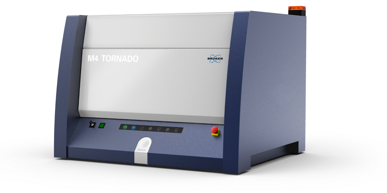
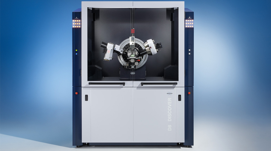
With the D8 DISCOVER Family and D8 ADVANCE Plus, Bruker offers a broad range of XRD solutions to address the requirements of the semiconductor market in research and development.
DIFFRAC.LEPTOS, Bruker‘s powerful thin film analysis suite, allows simultaneous refinement of XRR and HRXRD data to maximize information yield.
Micro-XRF
The decreasing thickness of functional layers makes meaningful measurement of the coating thickness a very challenging task. Micro-XRF can measure thicknesses ranging from single digit nm to tens of micrometers, depending on the present elements. For materials with high sensitivity, even sub-monolayers can be analyzed, with usually the deposited mass per area being measured instead of the thickness.