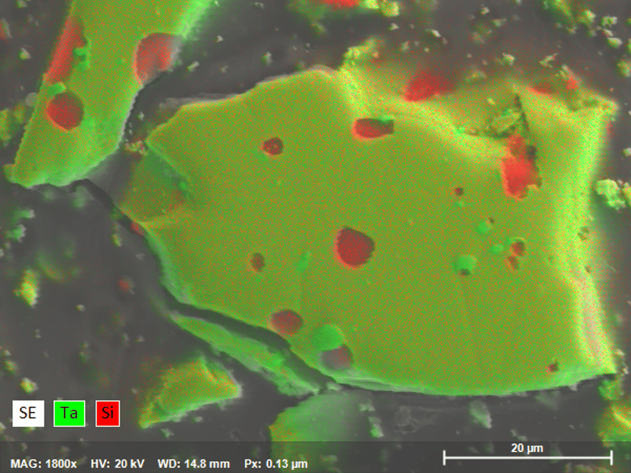
半导体微芯片材料的元素识别
导电陶瓷材料钨硅化物常用于微电子材料,如微芯片。钨硅化物也可能作为半导体材料中的耐火相,如硅片上的钨硅化物。
为了在质量控制中实现微和纳米水平的高空间分辨率,材料必须以低加速电压进行分析,而这个前提使这些物相的识别变得困难。在这个例子中,W M 线系的谱峰可以被激发,而这些谱峰会与基板材料 Si K+线系发生严重重叠。
由此产生的主要元素(Si)的 EDS 峰值会变宽,并掩盖了第二物相(W)的存在。相对应的,如果使用 QUANTAX WDS 进行分析,由于其卓越的能量分辨率,W 和Si 的每个峰都可以被完美识别。

WDS 采集的电子芯片上 Si 和W 元素的分布图

在1.6-2.0 keV 能量范围内,硅化钨材料毫无重叠的谱峰展现了WDS 的高能量分辨率
Alternatives to Wavelength Dispersive Spectroscopy
QUANTAX WDS is no longer available to purchase. However, we have suitable alternatives that cover the benefits of WDS - light element detection, peak deconvolution, trace element detection and efficient X-ray line separation.
To learn more about these solutions view our page Analytical Alternatives to Wavelength Dispersive Spectroscopy.
Information about the end of sales and service lifetime of QUANTAX WDS and XSense can be found here.