Opto LED
LED-Epi-Schichtuntersuchung
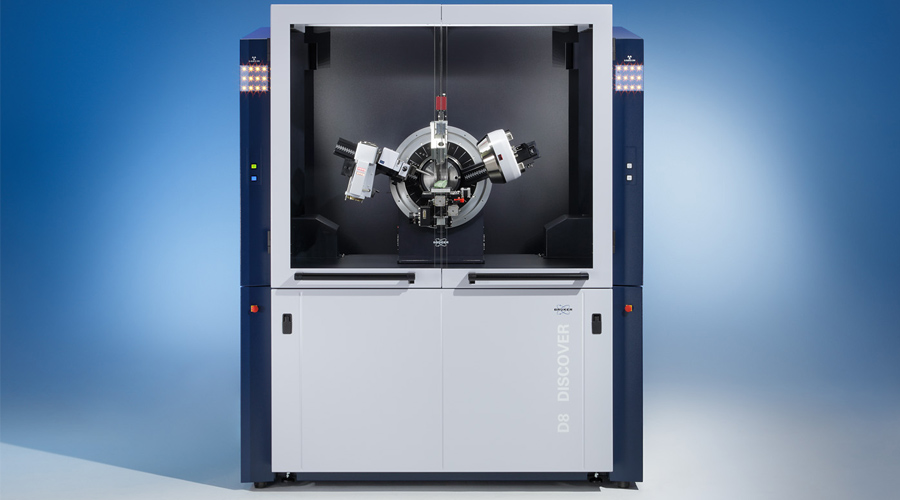
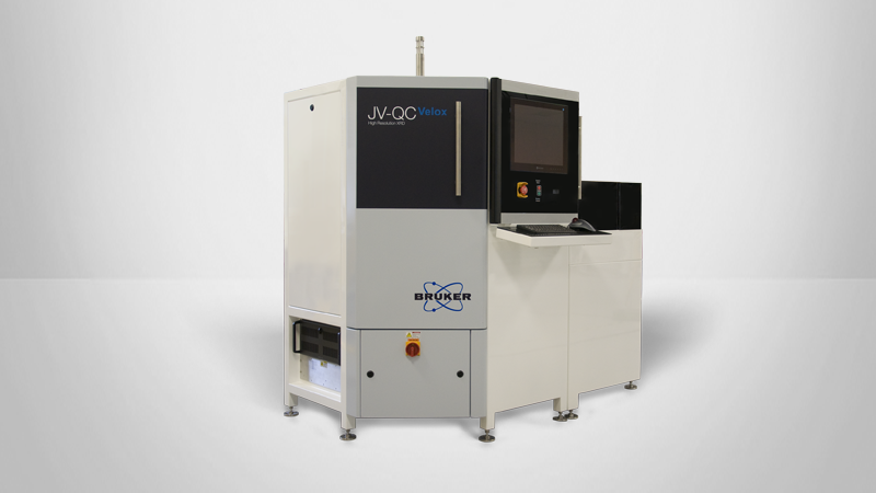
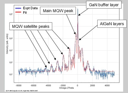
HRXRD ist für die Messung von Epi-Schichten gut etabliert. Das Bruker QCVelox-E das modernste und führende Gerät auf dem Gebiet der LED-Untersuchung und wird in der gesamten Branche eingesetzt.
Das QCVelox-E ermöglicht vollautomatische HRXRD-Messungen mit hohem Durchsatz, zusammen mit einer automatischen RADS-Analyse und der Erstellung von Ergebnisberichten, so dass die Kunden ihren Prozess auch ohne die Hilfe von Röntgenexperten bei der Datenauswertung überwachen können. Die optionale, ab Werk bereitgestellte SECS-GEM-Host-Software und die Roboterbeladung vervollständigen die Automatisierung des Systems.
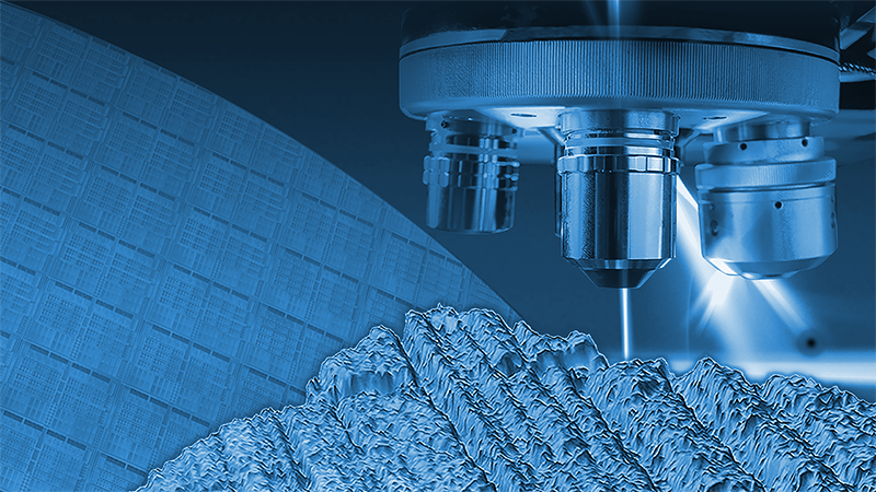
Improving Patterned Sapphire Substrate Performance and Yield
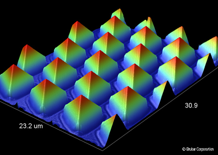
Understanding nanoscale dimensions of patterned sapphire substrates (PSS) are critical for next-generation materials development and to maintain production quality. Bruker's 3D Optical Profilers provide fast, accurate measurement of height, pitch and diameter of PSS features.
Extensive automation features enable operator-independent metrology of numerous sites so that process variations across wafers can be well understood and controlled.
In addition, optical profilers and stylus profilers are used to characterize the roughness, thickness and shape of phosphor layers which are used to create white light from an underlying blue LED. These properties have a large affect on the efficiency of light conversion, and can also affect the color and uniformity of illumination.
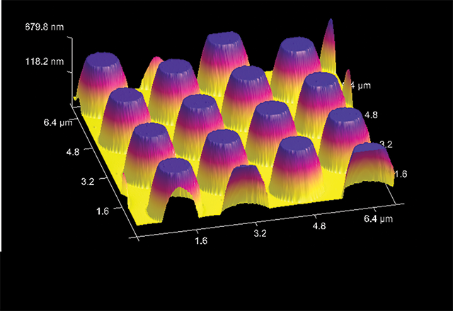
Sub-Nanometer Metrology of PSS Structures
As the pitch of patterned sapphire substrate goes below 2 microns, where optical techniques cannot achieve the resolution needed to provide valuable process metrology, atomic force microscopes (AFM) deliver an accurate solution. They provide sub-nanometer resolution and the ability to measure all the data necessary to keep the PSS manufacturing process under control.
Körnerstruktur- und Elementaranalyse

Die Elektronenmikroskop-Analysatoren von Bruker, wie das EDS für SEM und TEM, EBSD, WDS und Mikro-RFA, ermöglichen die Analyse der Textur (EBSD) und der Elementverteilungen bis in den ppm-Bereich mit hoher räumlicher Auflösung und auch in geschichteten Materialien (Mikro-RFA). Besonders schnelle Analysen, wie sie in der Qualitätskontrolle oder bei großen Probenbereichen benötigt werden, sind mit einem Gerät mit hohem Sammelwinkel, wie dem Bruker-Detektor XFlash FlatQUAD, möglich.
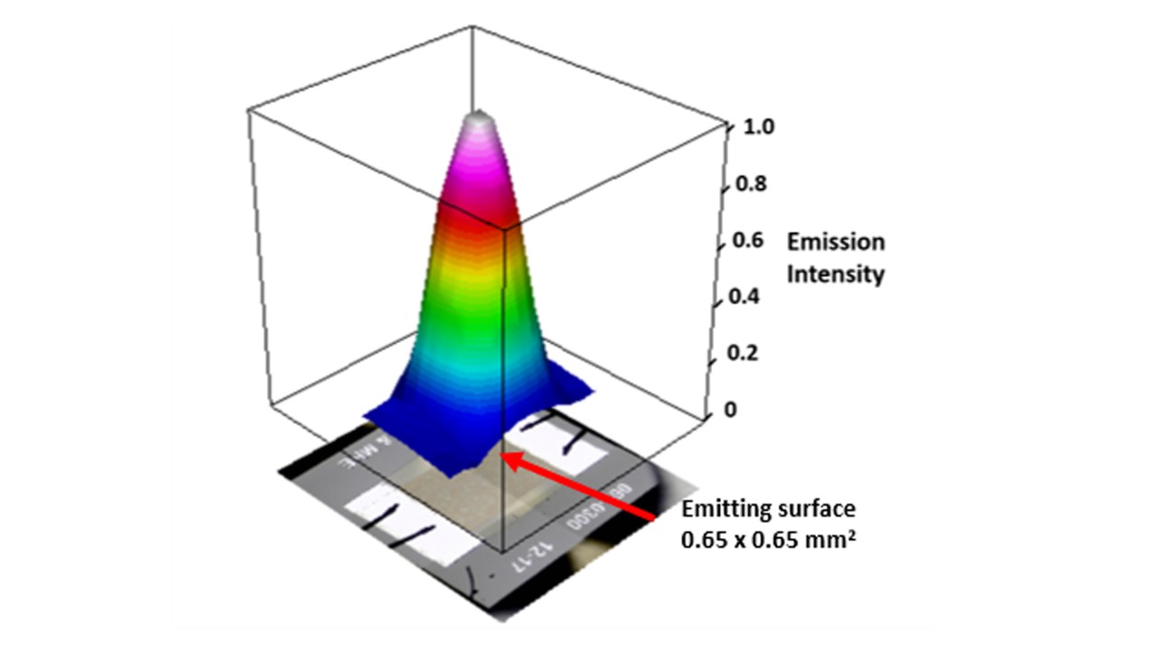
Laser and LED Emission, Electroluminescence
FT-IR emission spectroscopy is the ideal tool to analyze novel IR sources, lasers, LEDs or electroluminescence. Highest spectral resolution of the research series FT-IR spectrometers allows completely resolving the laser modes. Time-resolved measurement with temporal resolution down to the low ns range enables the acquisition of single laser pulses. Amplitude-modulated step scan making use of lock-in technique offers a possibility to record very weak emission signals. For small emitters in mm or µm range an IR microscope adapted to a research spectrometer provides excellent lateral resolution and utmost sensitivity for emission microscopy at the same time.
Detector Testing and Characterization by FT-IR
Self-developed infrared detectors can be tested and characterized with Bruker FT-IR research spectrometers. Single element detectors may be directly adapted to external optics of the research series spectrometers. For characterization of focal plane array (FPA) detectors dedicated external measurement modules are available.