Opto LED
LED Epi Layer Monitoring
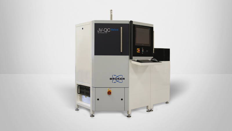
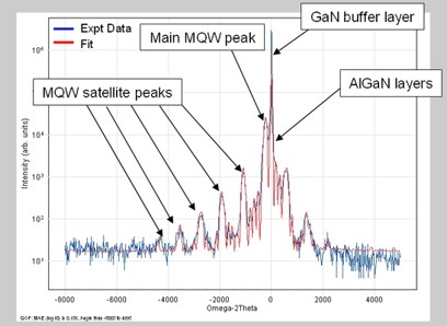
HRXRD is well established for the measurement of epi-layers. The Bruker QCVelox-E is the state of the art leader in LED monitoring and is widely used throughout the industry.
The QCVelox-E enables fully automated, high throughput HRXRD measurements, along with automatic RADS analysis and reporting of the results to enable customers to monitor their process without needing X-ray experts to analyze data. Optional SECS-GEM factory host software and robot loading are available to complete the automation of the system.
Improving Patterned Sapphire Substrate Performance and Yield
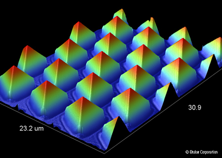
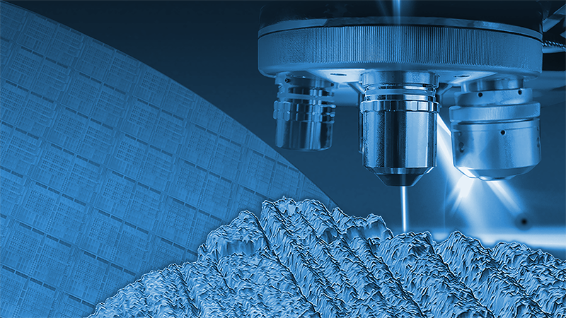
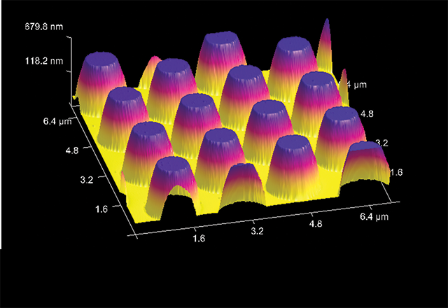
Understanding nanoscale dimensions of patterned sapphire substrates (PSS) are critical for next-generation materials development and to maintain production quality. Bruker's 3D Optical Profilers provide fast, accurate measurement of height, pitch and diameter of PSS features.
Extensive automation features enable operator-independent metrology of numerous sites so that process variations across wafers can be well understood and controlled.
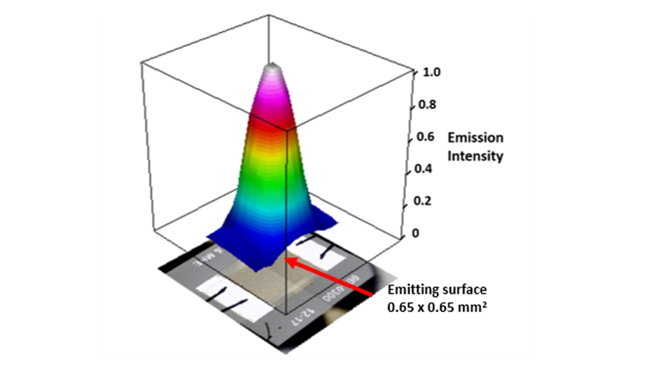
In addition, optical profilers and stylus profilers are used to characterize the roughness, thickness and shape of phosphor layers which are used to create white light from an underlying blue LED. These properties have a large affect on the efficiency of light conversion, and can also affect the color and uniformity of illumination.
Sub-Nanometer Metrology of PSS Structures
As the pitch of patterned sapphire substrate goes below 2 microns, where optical techniques cannot achieve the resolution needed to provide valuable process metrology, atomic force microscopes (AFM) deliver an accurate solution. They provide sub-nanometer resolution and the ability to measure all the data necessary to keep the PSS manufacturing process under control.
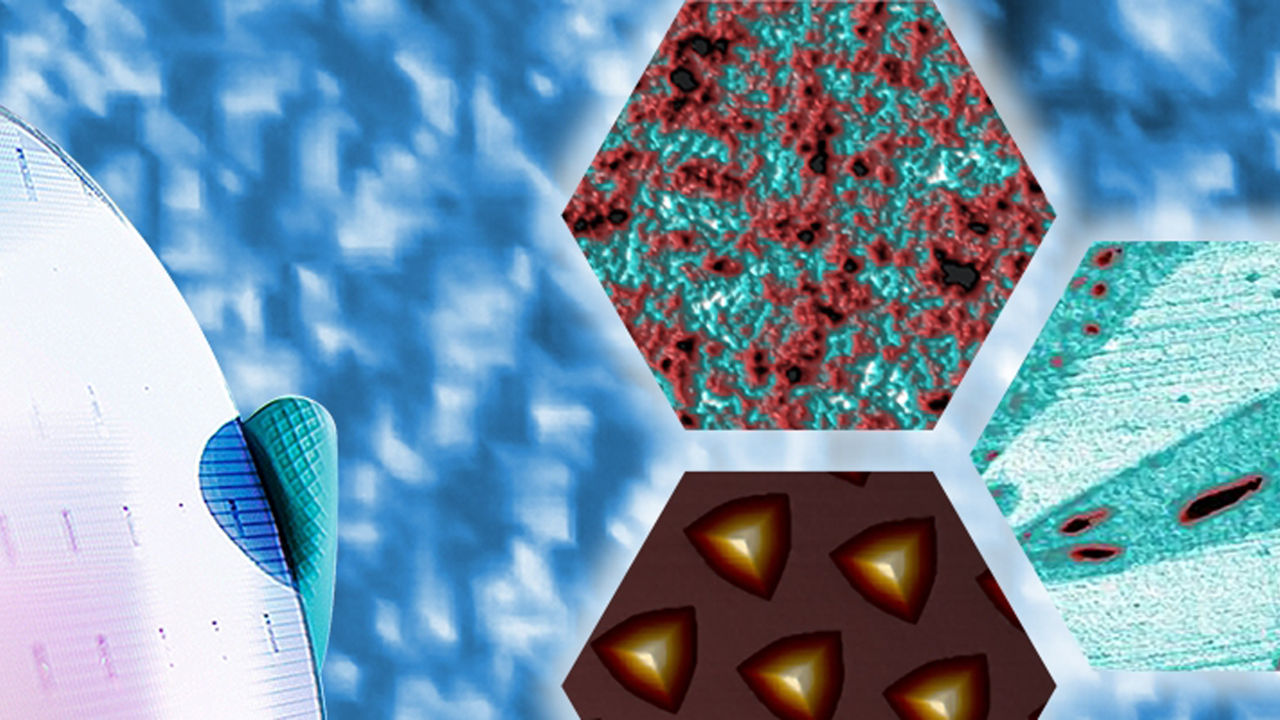
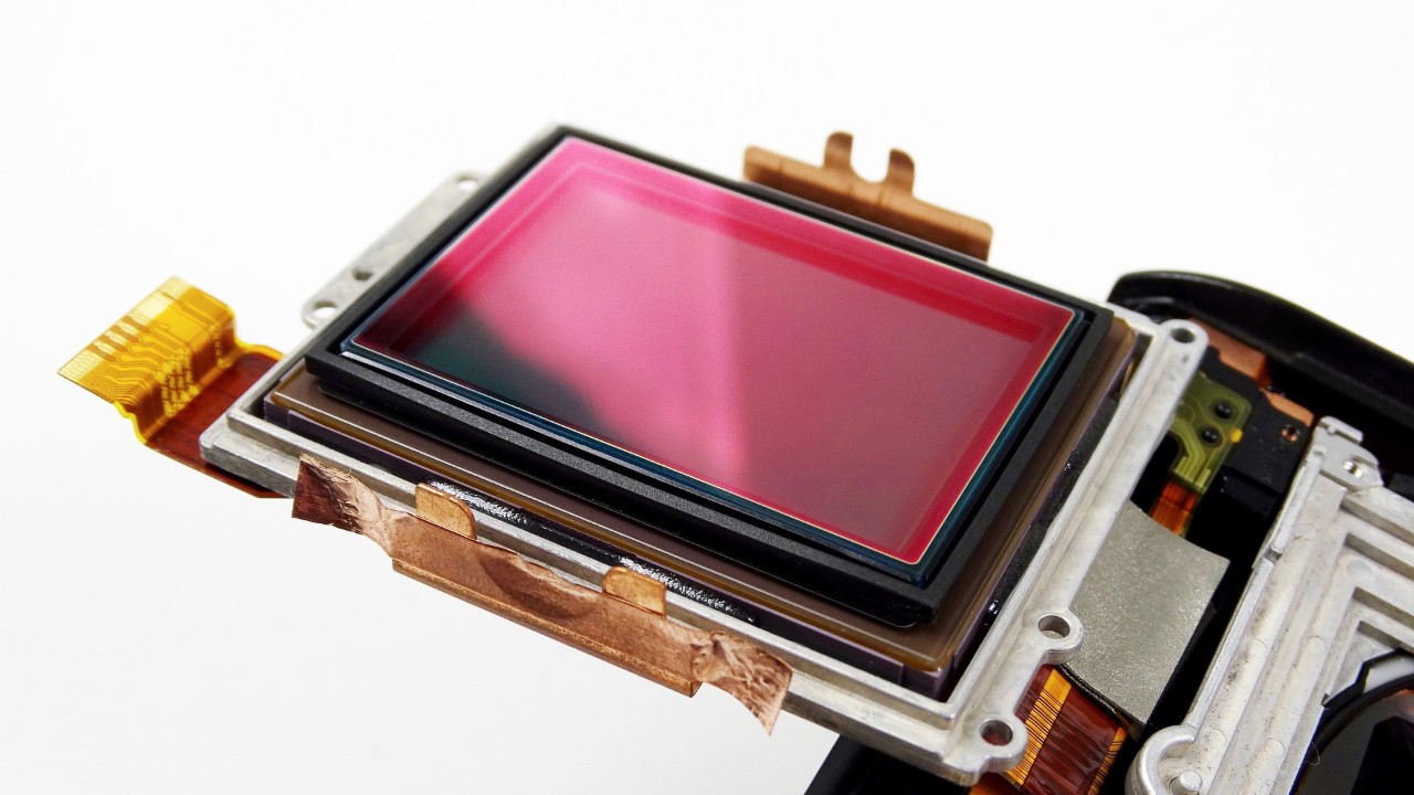
Grain Texture and Elemental Analysis of Optoelectronic Devices

Understanding features on nano to micro meter scales in elemental composition and crystallographic properties is a requirement to understand performance and behavior of modern optoelectronic devices. Bruker provides a variety of electron microscope analyzers to investigate those properties on SEM and TEM systems. Bruker's electron microscope analyzers, such as EDS for SEM and TEM, EBSD, WDS and Micro-XRF, allow the analysis of texture (EBSD) and the element distributions down to ppm with high spatial resolution and also in layered materials (Micro-XRF). Particularly fast analysis, such as needed in quality control or for large sample areas, is possible using a high collection angle device, such as the Bruker XFlash® FlatQUAD detector.
Laser and LED Emission, Electroluminescence
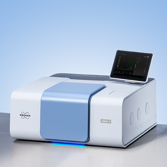
FT-IR emission spectroscopy is the ideal tool to analyze novel IR sources, lasers, LEDs or electroluminescence. Highest spectral resolution of the research series FT-IR spectrometers allows completely resolving the laser modes. Time-resolved measurement with temporal resolution down to the low ns range enables the acquisition of single laser pulses. Amplitude-modulated step scan making use of lock-in technique offers a possibility to record very weak emission signals. For small emitters in mm or µm range an IR microscope adapted to a research spectrometer provides excellent lateral resolution and utmost sensitivity for emission microscopy at the same time.
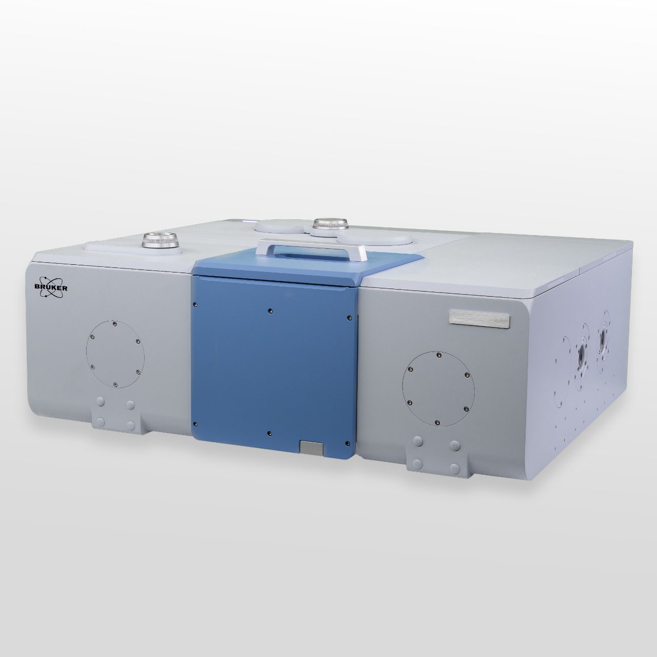
Detector Testing and Characterization by FT-IR
Self-developed infrared detectors can be tested and characterized with Bruker FT-IR research spectrometers. Single element detectors may be directly adapted to external optics of the research series spectrometers. For characterization of focal plane array (FPA) detectors dedicated external measurement modules are available.