Surface Characterization of Semiconductors Workshop [2021]
See how Bruker instruments are supporting cutting-edge manufacturing today and the development of <3 nm nodes for future applications.
Watch this workshop to discover our full range of high-performance metrology tools and techniques for the surface characterization of semiconductor materials and devices. In a series of six expert-led presentations, viewers will see our instruments in action and discover how materials scientists and engineers can — and do — use them to better understand the properties of semiconductor materials and their behavior at the nanoscale. Presentations include:
- In-depth discussions of innovative and everyday characterization techniques for both R&D and production;
- Real-time demonstrations of Bruker's high-resolution, in-situ scanning probe microscopy (SPM) imaging and high-speed mechanical property mapping technology; and
- Expert answers to common questions posed by semiconductor researchers and engineers.
Webinar Summary
This workshop explores our full range of metrology solutions for semiconductor R&D and process control. Our semiconductor applications experts discuss and semonstrate a variety of processes, including:
- Nanomechanical property sampling;
- Nanoscale-to-microscale indentation;
- Surface roughness measurement;
- Chemical mechanical planarization (CMP); and
- Etch-depth characterization.
The information presented is ideal for researchers and engineers involved in R&D and the monitoring and improvement of manufacturing processes.
ON-DEMAND RECORDING |00:03:33]
Welcome, everybody, and thank you so much for joining today's virtual workshop on the surface characterization of semiconductors. Our event today is brought to you by Bruker Nano Surfaces and Metrology division of North America. My name is Mike Berg, I'll be your host today, and I am the nanoindentation Product Specialist for the Bruker Hysitron business unit in Minneapolis.
We've got an exciting program today for everyone with a number of our applications experts joining to share about Bruker technologies and their applications, and to answer your questions.
Before we get started with the program, I wanted to bring up a few housekeeping items. Today's event is being recorded, so you will all be receiving a follow up email so you can view the on demand content afterwards. Feel free to share this with your colleagues or go back and rewatch sections of interest or that you may have missed.
We're encouraging you to submit your questions at any time during the talks. Each of our talks will have approximately 20 minutes, and then we'll reserve around five minutes for Q&A on each talk. You can submit your questions in the "Question" box of the GoToWebinar meeting dashboard, and for the questions we don't have time to address after each of the tal, we'll have an end-of-session Q&A in which we'll try to get to all of the questions. Otherwise, you can also write in directly by email after the event. You also have the flexibility to resize your webcam screen, as well as the presentation screen, so feel free to use those features.
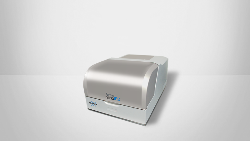
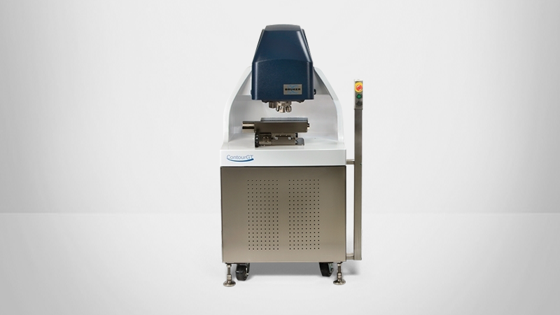
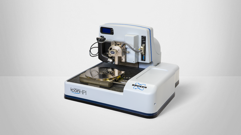
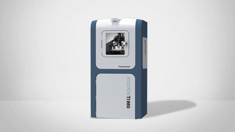
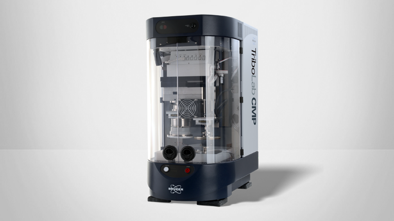
Before we get to the agenda, I just wanted to also point out that we will be featuring a number of technologies from the Bruker Nano Surfaces product portfolio in the talks today, starting with the high resolution Dimension HPI atomic force microscope, then the Anasys nanoIR3 spectrometer, the Hysitron TI 980 nanoindenter for nanoindentation and no scratch, the Contour GT-X optical profiler, the DektakXT stylus profiler, the TriboLab CMP tribometer, and, lastly, the Insight CAP HP automated AFM metrology tool.
So just a quick summary of our program today:
- Our first talk will be on AFM applications for semiconductors, including automation, metrology and advanced techniques by John Thornton, from our Boston Area Bruker office.
- Then we'll move to the Santa Barbara, California Office, we're Cassandra Phillips will be talking about nanoscale chemical analysis of contaminants using photothermal AFM-IR.
- We'll move over then to our Minneapolis area office, we're Douglas Stauffer will be speaking about mechanical characterization of semiconductor samples and devices with the nanoindentation instruments.
- Then over to the Boston area office, again, where Sandeep Basu will be speaking about semiconductor 3D metrology using optical and stylus profiling.
- Then we will move to the San Jose office where Kora Farokhzadeh will be talking about the TriboLab CMP bridging the gap between bench-scale research commercial manufacturing.
- And, finally, also from the San Jose office, Ingo Schmitz will be presenting on the automated surface characterization of semiconductor wafers for yield management.
| Length | Topic | Presenter |
| 26 min | AFM applications for semiconductors, including automation, metrology and advanced techniques | John Thornton |
| 23 min | Nanoscale chemical analysis of contaminants using photothermal AFM-IR | Cassandra Phillips, Ph.D. |
| 26 min | Mechanical characterization of semiconductor samples and devices with the nanoindentation instruments | Douglas Stauffer, Ph.D. |
| 28 min | Semiconductor 3D metrology using optical and stylus profiling | Sandeep Basu, Ph.D. |
| 36 min | TriboLab CMP bridging the gap between bench-scale research commercial manufacturing | Kora Farokhzadeh, Ph.D. |
| 34 min | Automated surface characterization of semiconductor wafers for yield management | Ingo Schmitz, Ph.D. |
Featured Products
Featured Technology
Speakers

John Thornton,
Senior Applications Scientist, BrukerJohn Thornton is a Senior Applications Engineer at Bruker Nano Surfaces with 25+ years of experience in the field of Atomic Force Microscopy (AFM). He learned AFM at North Carolina State University in the 1990s, and then joined Digital Instruments, a pioneering company in early AFM development, and continued with the company through acquisitions by Veeco Instruments, and then Bruker. John has co-authored many scientific publications and developed scanning probe microscopy training courses. Currently, John spends a significant amount of time running AFMs and educating others on techniques. He currently works from his home in Virginia, and from the Bruker AFM applications lab in Billerica, MA.

Cassandra Phillips, Ph.D.
Senior Product Manager, BrukerCassandra did her Ph.D. at the University of Toronto exploring the photophysics of boron nitride nanotubes using scattering scanning nearfield optical microscopy (s-SNOM) and computational models. She has been working at Bruker Nano Surfaces and Metrology since September 2019 as an Applications Scientist focusing on nanoscale IR spectro-microscopy and other correlated imaging techniques realized with atomic force microscopy.

Douglas Stauffer, Ph.D.
Senior Manager of NI Applications Development
Douglas Stauffer, Ph.D. is the Senior Manager for Applications Development for the Hysitron product lines at Bruker Nano, Inc. In short, he manages the internal testing laboratory, engages in collaborations, and assists with sales-related activities with respect to nanomechanical testing techniques. He works with a wide variety of professionals in his role, ranging from professors studying incipient events at very small length scales to industrial manufacturing of 300mm wafers for logic and memory
His current research focus is on developing new techniques for understanding structure and processing relationships with regard to nanomechanical performance. These relationships and techniques can then be applied to a wide range of applications that include both applied and fundamental studies for assessing component and microstructure capabilities to resist failure. These techniques include in and ex-situ testing and the development of in operando type experiments, to gain insight into the role that plasticity and fracture play in the varying failure regimes under operating conditions.
Douglas received his Ph.D. in Materials Science from the University of Minnesota in 2011. He then joined the R&D department as a Senior Staff Scientist working in instrumentation and applications at Hysitron. Hysitron was acquired by Bruker Nano in January 2017.

Sandip Basu, Ph.D.
Application Scientist, BrukerSandip Basu is an applications scientist at Bruker Nano Surfaces and Metrology division, where he works extensively on nano-mechanical and nano-tribological behavior of coatings and thin films, along with surface texture analysis using white light interferometry and stylus profilometry. He has obtained his Ph.D. in Materials Science and Engineering from Drexel University and has been involved in the industry for more than 10 years developing and promoting applications for nano-scale surface metrology.

Kora Farokhzadeh, Ph.D.
Application Scientist, Bruker
Kora is an application scientist in Bruker’s Tribology, Stylus, and Optical Metrology Group. She got her start in tribology as a graduate student in Materials Engineering, University of Windsor, Ontario, where she focused on dry sliding wear behavior of titanium alloys. She continued that subject into her doctoral studies to investigate surface engineering of titanium alloys for simultaneous wear and fatigue improvements. Later as a post-doc, her work experience can be summarized as surface engineering subjects, including design and fabrication of erosion- and corrosion-resistant cermet thermal spray coatings, wear-resistant polymer composite coatings, and protective coatings for automotive engine applications. Kora’s current role at Bruker lies at the forefront of innovative tribology testing techniques tailored for application, involving wear resistance and friction assessment, screening materials and surfaces by scratch testing and indentation hardness, and analysis of lubricants’ performance for a variety of automotive, biomedical and microelectronics applications. As part of her work, she is an affiliated graduate faculty at Southern Illinois University, collaborating on introducing a new benchtop technique to evaluate the behavior of friction brake materials.

Ingo Schmitz, Ph.D.
Technical Marketing Engineer, Bruker
Ingo Schmitz received his Ph.D. in Chemistry from the University of Technology, Vienna Austria in 1996. His Ph.D. work focused on the development of SPM-based in-situ characterization of corrosion processes of glass and metal surfaces. Since 1997, Ingo Schmitz works at Bruker (formerly Digital Instruments & Veeco Instruments) in both Santa Barbara, USA. At Bruker, he held positions as an R&D engineer and application development scientist and contributed in the development of SPM methods including automated surface characterization of polysilicon. Currently, he is working in the technical marketing of automated AFM systems.