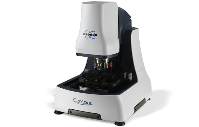
3D Optical Profilometer

ContourX-200

Flexible benchtop for surface texture metrology

ContourX-200

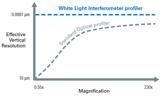
The ContourX-200 Optical Profilometer provides the perfect blend of advanced characterization, customizable options, and ease of use for best-in-class fast, accurate, and repeatable non-contact 3D surface metrology. The gage-capable, small footprint system offers uncompromised 2D/3D high-resolution measurement capabilities using a larger FOV 5 MP digital camera and new motorized XY stage. Boasting unmatched Z-axis resolution and accuracy, the ContourX-200 provides all the industry recognized advantages of Bruker’s proprietary white light interferometry (WLI) technology without the limitations of conventional confocal microscopes and competing standard optical profilers.

Automation
capabilities
Enable routines for faster measurement and analysis.
Motorized
XY stage
Provides low-noise, high-speed operation for quantitative metrology.
Vibration-tolerant
compact design
Delivers measurement stability and gage-capable repeatability.
Features

Uncompromised, Best-in-Class Metrology

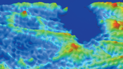
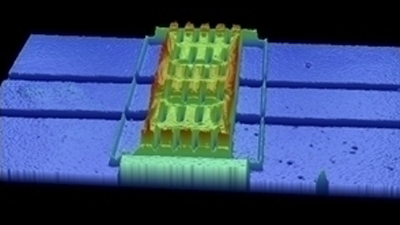
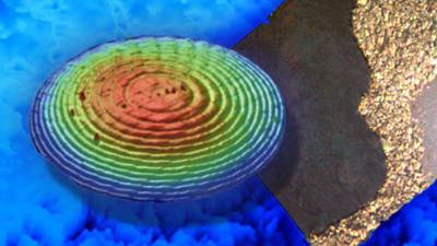
Built upon over four decades of proprietary WLI innovation, the ContourX-200 optical profilometer exhibits the low noise, high-speed, accuracy, and precision results that quantitative metrology requires. With the use of multiple objectives and integrated feature recognition, features can be tracked over a variety of fields of view and at sub-nanometer vertical resolution, providing scale-independent results for quality control and process monitoring applications in very diverse industries. ContourX-200 is robust in all surface situations from 0.05% to 100% reflectivity. New hardware features include an innovative stage design for larger stitching capabilities and a 5MP camera with a 1200x1000 measurement array for lower noise, larger field-of-view, and higher lateral resolution.

WLI offers constant and ultimate vertical resolution for all objectives.

Widest Application Analysis Capabilities

ContourX-200 motorized stage.

Utilizing powerful VisionXpress and Vision64 user interfaces, the ContourX-200 offers thousands of customized analyses for productivity in labs and on the factory floors. Bruker’s new Universal Scanning Interferometry (USI) measurement mode provides fully automated, self-sensing surface texture, optimized signal processing while delivering the most accurate and realistic computation of the surface topography being analyzed. The larger FOV provided by the system’s new camera and flexibility afforded by the new motorized XY stage enables more flexibility and higher throughput for a broad range of samples and parts. The hardware and software combine to provide streamlined access to top optical performance, completely outclassing comparable metrology capabilities.

Applications

Surface-Independent Metrology with Application-Specific Solutions

Precision Engineering

Keep the surface texture and geometric dimensions of precision-engineered parts within tight specification limits. Our gage-capable measurement systems provide efficient feedback and reporting as you monitor, track, and evaluate processes and assess GD&T conformance.

MEMS and Sensors

Perform high-throughput, highly repeatable etch depth, film thickness, step-height, and surface roughness measurements, as well as advanced critical dimension metrology of MEMS and optical MEMS. Optical profiling can characterize devices throughout the manufacturing process from wafer to final test, and even through transparent packaging.

Orthopedics/Ophthalmics

Obtain precise, repeatable measurements of implant materials and components through the complete product life cycle. Our WLI optical profilers support R&D, QA, and QC analyses, for applications ranging from characterization of surface parameters of lens and injection molds to surface finish verification and wear of medical devices.

Tribology

Measure, analyze, and control the impact of friction, wear, lubrication, and corrosion on material/component performance and lifespans. Determine quantitative wear parameters and perform fast pass/fail inspections on the widest range of shiny, smooth, or rough surfaces.

Semiconductors

Improve yield and reduce costs for both front- and back-end manufacturing processes with automated, non-contact, wafer-scale metrology systems. Perform post-CMP die flatness inspection; bump height, coplanarity, and defect identification and analysis; and measure the critical dimensions of component structures.

Optics

Better understand the root causes of defects and optimize polishing and finishing processes with accurate and repeatable sub-nm roughness measurements. Our non-contact metrology systems enable compliance with increasingly stringent specifications and ISO norms for samples ranging from small aspheric and free-form optics, to optical components with complex geometries, to diffraction gratings and microlenses.

Contact Us

Input value is invalid.

* Please fill out the mandatory fields.

Please enter your first name
Please enter your last name
Please enter your e-mail address
Please enter a valid phone number
Please enter your Company/Institution
What best describes your current interest?
Join our email subscription list to receive related webinar invitations, product announcements, and information about upcoming events near you.
Please accept the Terms and Conditions