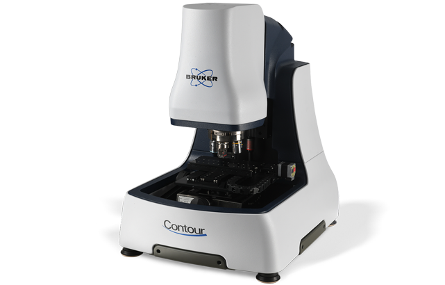
三维光学轮廓仪

ContourX-200

ContourX家族中的高效能台式光学轮廓仪,配备自动XYZ样品台,高级查找表面功能,拼接及大范围成像功能

ContourX-200

ContourX-200 光学轮廓仪提供了高级表征能力、可选定制配件、和使用方便三者的完美融合,是同类产品中最快、最准确、可重复性最高的非接触式三维表面计量系统。该计量系统占地面积小,采用更大视场、5MP 数码摄像头和全新电动 XY 工作台,具有卓越的二维/三维高分辨测量能力。ContourX-200 拥有出色的 Z 轴分辨率和精确度,具备布鲁克专有白光干涉(WLI)技术广受业界认可的所有优势,而且不存在传统共聚焦显微镜和同类普通光学轮廓仪的局限性。

自动化
能力
可实现更快测量和分析速度的程序。
电动
XY 工作台
实现低噪声高速定量计量。
耐振动
紧凑设计
提供稳定、可重复的测量。
特点

同类最佳计量技术

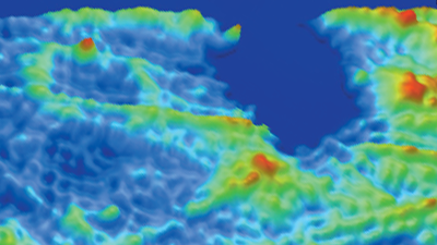
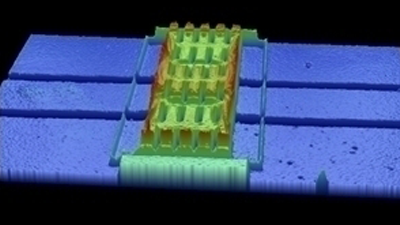
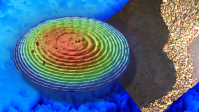
ContourX-200 光学轮廓仪依托 40 多年的 WLI 自主创新成果,可满足定量计量所需的低噪声、高速、准确度和精确度。通过使用多种物镜和图案识别,可以亚纳米垂直分辨率在多个视场跟踪特征,为多个行业的质量控制和过程监控应用提供不受尺寸大小影响的结果。ContourX-200 在反射率 0.05% 到 100% 的所有表面情况下都能发挥稳定性能。新增硬件特点包括为获取更大拼接而创新设计的工作台;一只 5MP 摄像头,采用 1200x1000 测量阵列,实现低噪声、更大视场和更高横向分辨率。

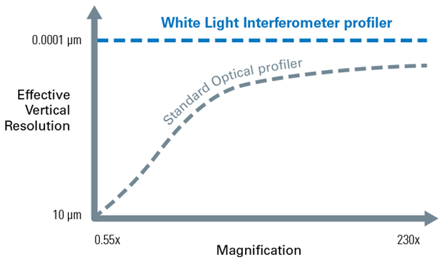
白光干涉所有物镜均提供恒定的最佳垂直分辨率。

最广泛的应用分析能力

轮廓X-200电动级。

ContourX-200 采用强大的 VisionXpress 和 Vision64 用户界面,提供数千种自定义分析以提升实验室和工厂的效率。布鲁克全新通用扫描干涉(USI)测量模式可提供全自动、自感知表面纹理、优化信号处理,同时对所分析的表面形貌执行最准确、最实际的计算。该系统采用新款摄像头,扩大了视场,加上新型电动 XY 工作台具有的灵活性,提升了处理多种样品和零部件时的灵活性和效率。软硬件的完美结合,实现卓越的光学性能,全面超越同类计量技术。

应用

Surface-Independent Metrology with Application-Specific Solutions

Precision Engineering

Keep the surface texture and geometric dimensions of precision-engineered parts within tight specification limits. Our gage-capable measurement systems provide efficient feedback and reporting as you monitor, track, and evaluate processes and assess GD&T conformance.

MEMS and Sensors

Perform high-throughput, highly repeatable etch depth, film thickness, step-height, and surface roughness measurements, as well as advanced critical dimension metrology of MEMS and optical MEMS. Optical profiling can characterize devices throughout the manufacturing process from wafer to final test, and even through transparent packaging.

Orthopedics/Ophthalmics

Obtain precise, repeatable measurements of implant materials and components through the complete product life cycle. Our WLI optical profilers support R&D, QA, and QC analyses, for applications ranging from characterization of surface parameters of lens and injection molds to surface finish verification and wear of medical devices.

Tribology

Measure, analyze, and control the impact of friction, wear, lubrication, and corrosion on material/component performance and lifespans. Determine quantitative wear parameters and perform fast pass/fail inspections on the widest range of shiny, smooth, or rough surfaces.

Semiconductors

Improve yield and reduce costs for both front- and back-end manufacturing processes with automated, non-contact, wafer-scale metrology systems. Perform post-CMP die flatness inspection; bump height, coplanarity, and defect identification and analysis; and measure the critical dimensions of component structures.

Optics

Better understand the root causes of defects and optimize polishing and finishing processes with accurate and repeatable sub-nm roughness measurements. Our non-contact metrology systems enable compliance with increasingly stringent specifications and ISO norms for samples ranging from small aspheric and free-form optics, to optical components with complex geometries, to diffraction gratings and microlenses.

联系我们

Input value is invalid.

* 请填写必填字段。

请输入您的姓名
请输入您的姓氏
请输入您的电子邮件地址
请输入您的公司/机构
您目前所处的阶段是
是否订阅电子邮件,以便收到网络研讨会邀请、产品公告和近期的活动。
请接受条款和条件