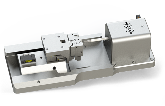
Hysitron PI 80
Hysitron PI 80 SEM PicoIndenter
Bruker’s PI 80 SEM PicoIndenter is a depth-sensing nanomechanical test instrument specifically designed to augment the imaging capabilities of scanning electron microscopes (SEM, FIB/SEM, PFIB). With this base nanoindentation tool, it is possible to perform quantitative in-situ nanomechanical testing while simultaneously imaging with the SEM. Featuring Bruker’s industry-leading capacitive transducer, PI 80 provides exceptional performance and superior stability at the nanoscale. Its compact, low-profile design makes the instrument ideally suited for small-chamber SEMs, as well as standalone Raman and optical microscopes, beamlines, and more. With its combination of features, testing modes, and optional accessories, the PI 80 SEM PicoIndenter offers an excellent introduction to advanced nanomechanical property testing inside your SEM.
To learn more, continue reading, download the datasheet, or see FAQs about this product.
In-Situ Mechanical Data Synchronized with SEM Imaging
In-situ mechanical data acquired with the Hysitron PI 80 is synchronized with SEM imaging and displayed in side-by-side video format. Simultaneous mechanical measurements and SEM data enables a more complete understanding of material deformation behavior. In the example at left, discontinuities in the load-displacement data are correlated to the onset of fracture observed in a FIB-milled beam containing copper interconnects and brittle dielectric material.
Designed to Augment Your SEM
With the compact form of Bruker’s capacitive transducer, Hysitron PI 80 can be mounted directly onto the SEM stage without being a permanent fixture in the microscope. The sample positioning stages accommodate samples up to 20 mm thick while providing precise sample positioning across more than 3 mm in all three directions (XYZ). In addition, the mechanical coupling of the sample stage and the transducer provides a stable, rigid platform for nanomechanical testing. Overall, this in-situ instrument enables stage tilt and working distance optimized for complementary SEM imaging and standard nanomechanical testing.
Expand PI 80 SEM's Capabilities
LEARN MORE:
Contact us for more information about available upgrade options and how PI 80 SEM can be configured to meet your specific measurement needs now and grow with your research going forward.
Watch our Recent Broadcasts on Nanomechanics in SEM
Our webinars cover best practices, introduce new products, provide quick solutions to tricky questions, and offer ideas for new applications, modes or techniques.
Frequently Asked Questions
PI 80 supports indentation, compression, bending, tension, fatigue, and electrical contact measurements. These modes enable quantitative nanomechanical property measurements of hardness, elastic modulus, yield strength, fracture toughness, creep exponent, and stress relaxation.
The instrument mounts directly to the SEM stage with a compact, low‑profile design suited to smaller chambers. A rigid mechanical coupling between stage and transducer supports stable testing while maintaining working distance and tilt.
PI 80 provides closed‑loop displacement control, closed‑loop load control, and open‑loop load control with a maximum load of 10 mN and up to 5 µm of displacement.
PI 80 offers a broad catalog of tips in multiple geometries and materials, including diamond, sapphire, vanadium carbide, boron nitride, tungsten, and steel.
Contact us to discuss what transducer and flexure options will be the best fit for your experiments.
Yes. You can request a quote using our online form, or contact us directly.
Contact Us About the Hysitron PI 80 SEM PicoIndenter
Ask us a question, request more information, or get in touch with a Bruker sales representative.
