
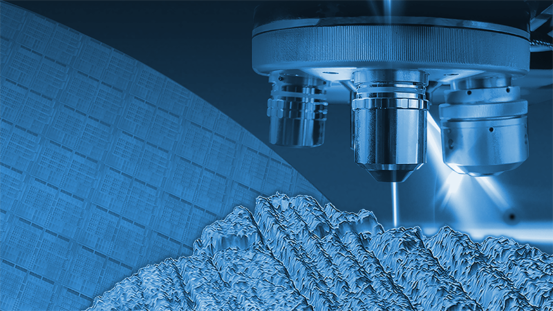
Bruker Solutions for Thin Film Characterization
Thin Film Instruments for Every Application
Film behavior is reflected in properties such as thickness, surface structure, optical response, chemistry, and mechanical performance. These properties are accessed using different types of metrology tools, depending on the measurement scale and sample. Bruker’s thin‑film metrology portfolio spans optical surface profiling and film metrology, contact profilometry, nanoscale surface and property imaging, nanoscale chemical analysis, and nanomechanical and tribological testing — covering thin‑film measurements from large‑area mapping to nanoscale and performance‑based evaluation.
AT-A-GLANCE
Common first‑pass techniques include:
- 3D optical profilometry: Rapid, non‑contact areal measurements for surface topography and texture (roughness/waviness) and step features
- Ellipsometry/reflectometry: Optical thickness and optical constants (n, k), including multilayer or optically complex films when optical property measurement or ultrathin sensitivity is the priority
- Stylus profilometry: Direct step height/thickness by contact, often used alongside optical methods to validate results and reduce ambiguity when contact is acceptable and higher confidence is required
It makes sense to add nanoscale or mechanical techniques when thickness and roughness values no longer explain what is happening — for example, when results look acceptable at larger scales but performance varies across domains, interfaces, or localized defects. In these cases, optical averages stop being explanatory, and additional methods are used to resolve structure, properties, or chemistry at the length scales that matter.
Common nanoscale property measurement techniques include:
- AFM: Nanometer‑scale topography and property contrast to reveal heterogeneity that can be invisible to optical methods
- nanoIR (AFM‑IR): Localized chemical identification and mapping when chemistry is driving performance differences and sub‑micron spatial resolution is required
- Nanomechanical testing: Hardness, modulus, adhesion, and fracture behavior at film‑relevant length scales to connect mechanical response to performance and reliability
It is often advisable to combine complementary techniques across scales to validate results across measurements, operators, and conditions and reduce ambiguity.
Single‑point measurements can be appropriate when films are expected to be uniform and the decision tolerates limited spatial sampling — for example, during quick checks, process trending, or reference validation.
Typical single‑point approaches include:
- Ellipsometry/reflectometry: Local thickness or optical properties at a defined site
- Stylus profilometry: Step height or thickness reference at a defined location when contact is acceptable
- Nanomechanical testing: Localized mechanical response at selected test sites when properties are part of the decision
Mapping or areal measurements are recommended when the area sampled affects whether the result can be trusted — for example, when non‑uniformity, gradients, localized defects, or heterogeneity influence yield, performance, or interpretation.
Typical mapping or areal approaches include:
- 3D optical profilometry (areal/stitched maps): Large‑area surface texture, roughness, waviness, and step/topography variation
- AFM/nanoIR (regional mapping): Nanoscale structure, property, or chemical variability across regions of interest
- Ellipsometry mapping: Thickness or optical property variation across wafers or panels
- Nanoindentation mapping: Mechanical property variation over large areas
In practice, mapping is often used to reveal spatial variability, followed by targeted measurements (either local spot checks for confirmation or higher‑resolution methods when additional detail or confidence is required).
When thickness and surface measurements are no longer sufficient to explain outcomes, additional techniques are used to connect structure and properties to behavior under load, during processing, or over time.
Common approaches include:
- Nanomechanical testing: Hardness, elastic modulus, adhesion, fracture, time-dependent deformation, and temperature-dependent response measured at film‑relevant length scales to relate mechanical response to performance and reliability while managing substrate influence
- Bulk scratch and tribology testing: Adhesion strength, friction, wear, critical load, and durability measured under representative contact conditions to evaluate coating robustness in real‑world applications
Thin‑film characterization workflows often combine complementary techniques to increase confidence and reduce ambiguity, especially when results will be used for process decisions, qualification, or failure analysis.
In practice, this may include:
- Pairing non‑contact optical methods (such as 3D optical profiling) with a direct reference measurement (such as stylus profilometry) to validate thickness or step height
- Using multiple measurement scales (areal mapping plus localized measurements) to confirm that results are representative
- Combining structural, chemical, and mechanical techniques to ensure that observed behavior is explained consistently across methods
Common Thin Films Applications/Measurement Needs
Thin film characterization starts with the question being asked. Different measurement needs — such as thickness, roughness, mechanical response, chemistry, or durability — emphasize different length scales, interactions, and levels of confidence. Selecting a technique based on the measurement need means considering what property matters most, over what area or scale it must be measured, and whether the goal is rapid screening, localized investigation, or defensible quantitative results.
This section organizes common thin‑film measurement challenges by application, reflecting the different types of questions that arise across thin‑film development, characterization, and process monitoring. Each application highlights the parameters being evaluated, the context in which they matter, and the type of information required to support reliable interpretation.
A given application may be addressed using one or more complementary characterization techniques, selected based on the film system and measurement requirements.
FIND THE RIGHT TECHNOLOGY FOR YOUR MEASUREMENTS:

Film Thickness & Uniformity
Core question(s): How thick is the film? How consistent is its thickness across the sample?
Importance: Film thickness (t) and thickness uniformity (Δt) are typically the first decision‑critical parameters evaluated in thin‑film workflows. They are used to confirm that a deposition or coating process is behaving as expected and to identify gradients or edge effects across wafers, panels, or substrates. Thickness consistency strongly influences yield, device performance, and confidence in downstream processing.
Technologies commonly used: 3D Optical Profilometry · Ellipsometry/Reflectometry

Surface Roughness & Texture
Core question(s): How rough is the film? How does its surface texture vary?
Importance: Surface roughness parameters such as Ra, Sa, Rq, and peak‑to‑valley height affect adhesion, friction, optical scatter, and long‑term reliability. Roughness and texture measurements are widely used for rapid screening of surface quality and for comparing materials or deposition conditions. Because these measurements are non‑destructive, they are often applied early and repeatedly throughout development and production monitoring.
Technologies commonly used: Stylus Profilometry · 3D Optical Profilometry · AFM

Step Height & Layer Thickness
Core question(s): What is the height difference between layers, features, or patterned regions?
Importance: Step height measurements provide a direct, absolute vertical distance between two surfaces, supporting determination of physical layer thickness in patterned, etched, or masked films. Metrics such as step height and trench depth are straightforward, geometry‑based values that are easy to interpret and correlate across tools and sites. These measurements are often used as reference checks to validate thickness obtained by indirect techniques.
Technologies commonly used: Stylus Profilometry · 3D Optical Profilometry · AFM

Optical Properties & Multilayer Response
Core question(s): What are the film's optical properties? How do they vary by material, thickness, or layer?
Importance: Optical properties such as refractive index (n) and extinction coefficient (k) define performance in optical coatings and optically functional thin films. These parameters support modeling of reflectance and transmission and are critical for interpreting thickness and behavior in multi-layer stacks. Optical measurements help connect material design to functional optical performance.
Technologies commonly used: Ellipsometry/Reflectometry

Nanoelectrical Properties & Behavior
Core question(s): What are the electrical properties of the film? How uniform are they across the sample?
Importance: Electrical behavior — such as local current, surface potential, or ferroelectric domain response — often defines thin‑film functionality. Nanoscale electrical measurements reveal spatial variability, domain structure, and process‑induced heterogeneity that are not captured by bulk or averaged measurements. These insights help correlate electrical performance with film structure, thickness, and processing conditions.
Technologies commonly used: AFM

Nanomechanical Properties & Behavior
Core question(s): How does my film respond mechanically at nanoscale length scales? Do these properties vary across the film?
Importance: Intrinsic mechanical properties such as hardness (H), elastic modulus (E), and adhesion govern durability and reliability in thin films. Because these properties can vary locally due to defects, domains, or microstructure, spatially-resolved measurements are used to identify heterogeneity. Nanomechanical testing connects film structure, locality, and mechanical behavior while minimizing substrate influence.
Technologies commonly used: Nanomechanical Testers · In-Situ Nanomechanical Testers · AFM

Chemical Composition at Small Scales
Core question(s): What is the film made of? How is chemistry distributed at the nanoscale?
Importance: Local chemical composition and nanoscale chemical heterogeneity often drive differences in electrical, mechanical, or optical behavior. Infrared absorption and spatially resolved chemical measurements reveal phase separation, interfacial chemistry, or compositional gradients that are invisible in bulk analysis. These insights support material understanding, failure analysis, and root‑cause investigations.
Technologies commonly used: AFM‑IR/NanoIR · AFM

Adhesion, Wear, & Durability
Core question(s): How resistant is the film to adhesion failure, wear, or mechanical damage? Will the film adhere and survive stress in-use?
Importance: Adhesion strength, wear rate, and coefficient of friction (CoF) determine whether thin films survive processing, repeated contact, and mechanical stress in use. These properties are especially critical for coatings where friction, abrasion, or loading can drive reliability limits. Adhesion and wear testing help define failure modes and durability margins.
Technologies commonly used: Tribology Testing · Nanomechanical Testing
Bruker Technology for Thin Films Characterization
With more than 50 years of innovation, Bruker is a trusted leader in surface characterization and metrology solutions. Bruker’s thin‑film measurement systems are designed to deliver accurate, reliable results and are supported by expert applications specialists.
Bruker’s thin film characterization portfolio spans non‑contact optical methods, contact‑based profiling, nanoscale imaging and spectroscopy, localized mechanical testing, and system‑level performance evaluation. Together, these technologies support the full thin-film workflow — from early research and process development to failure analysis and performance validation. Rather than relying on a single instrument, users can select from a broad set of tools optimized for different properties, scales, and stages of investigation.
Use this section to explore Bruker’s measurement platforms, including core capabilities, typical use cases, and how each technology is commonly applied in thin‑film characterization workflows.
FIND THE RIGHT TECHNOLOGY FOR YOUR MEASUREMENTS:
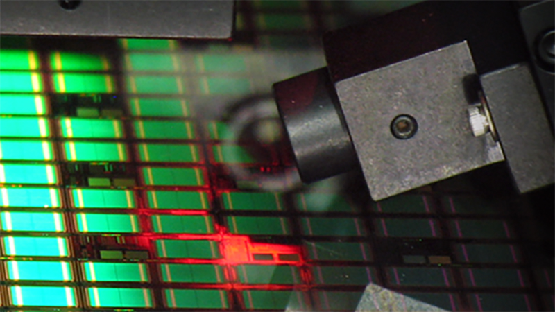
Optical & Surface Metrology Technologies
Optical and surface metrology technologies are commonly used to quickly characterize thin‑film thickness, surface texture, and uniformity. These methods are often the starting point for thin‑film workflows and provide critical context for deciding when additional validation or higher‑resolution analysis is needed.
About Our 3D Optical Profilers
Best used when you need:
- Fast, non‑contact insight into surface topography, roughness, waviness, or step features
- To screen large areas for thickness or uniformity variation before committing to higher‑resolution measurements
- To work with fragile, soft, or contact‑sensitive films where contact introduces risk
- To identify where variation exists and guide where higher‑resolution or contact techniques should be applied
What 3D optical profilometry provides:
3D optical profilometry uses white‑light interferometry to generate areal maps of surface height, roughness, waviness, and step features without contacting the film. By bringing the top surface and, when applicable, the substrate surface into focus, these measurements reveal surface structure and thickness variation across large areas where step features or exposed substrate are present.
In practice, optical profilometry is widely used for surface characterization, mapping, and process monitoring. It provides rapid insight into surface texture, step height, and thickness variation across wafers or panels, supporting screening, comparison, and process control. Measurement performance depends on film properties; very thick films can approach signal‑to‑noise limits, while thinner or translucent films may require optical modeling and refractive‑index input when thickness values must be tightly constrained.
Typical thin‑film questions 3D optical profiling answers:
- Is the film uniform across the wafer or substrate?
- Where does roughness, thickness, or topography variation exist?
- Are there surface features or step changes that indicate process non‑uniformity or drift?
Common uses in thin films applications include:
(See all 3D optical profilometry resources for thin film characterization here)
About Our Ellipsometry & Reflectometry Systems
Best used when you need:
- Film thickness with high sensitivity, including ultrathin and transparent films
- Optical constants (n, k) as part of the specification
- Insight into multilayer or optically complex stacks
- Non‑contact measurements supported by optical modeling
What ellipsometry/reflectometry provides:
Ellipsometry and reflectometry determine film thickness and optical properties by analyzing reflected light and fitting the response to optical models. These techniques are particularly powerful for transparent films, ultrathin layers, and multilayer stacks where optical response is as important as physical thickness.
By combining measured optical response with material models, ellipsometry and reflectometry enable precise thickness and optical‑constant extraction for well‑defined film systems. They are commonly used when optical properties directly affect performance or application requirements and when understanding layer‑by‑layer behavior in a stack is required.
Typical thin‑film questions it answers:
- What is the thickness of an ultrathin or transparent film?
- What refractive index or optical constants define this layer?
- How do individual layers contribute to the optical response of a stack?
- Is thickness variation optical, physical, or both?
Common uses in thin films applications include:
(See all ellispometry/reflectometry resources for thin film characterization here)
About Our Stylus Profilometers
Best used when you need:
- A direct, traceable step height or thickness value
- A reference measurement to validate non‑contact results
- Simple, easy‑to‑interpret data
- Contact is acceptable for the sample
What stylus profilometry provides:
Stylus profilometry measures surface height by mechanically tracing the surface with a probe. The resulting profile provides a direct physical measurement of step height or thickness that is straightforward to interpret.
In many workflows, stylus profilometry serves as a validation tool — confirming optical results, supporting model inputs, and reducing ambiguity when higher confidence is required. Because stylus profilometry provides a purely mechanical measurement, it is often used to confirm optical thickness results or to back‑calculate optical model parameters when non‑contact methods require refractive‑index assumptions.
Typical thin‑film questions it answers:
- What is the actual step height or film thickness at this location?
- Do optical measurements agree with a direct physical reference?
- Can I trust modeled or non‑contact results for this film system?
Common uses in thin films applications include:
(See all stylus profilometry resources for thin film characterization here)
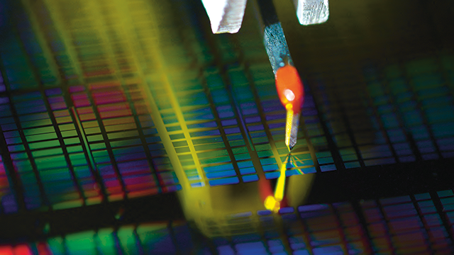
Nanoscale & Local Property Characterization Technologies
When thin‑film behavior cannot be explained by thickness or surface averages alone, nanoscale characterization techniques are used to investigate local structure, chemistry, and properties. These technologies provide insight at the length scales where interfaces, heterogeneity, and localized responses often drive performance.
About Our Atomic Force Microscopes
Best used when you need:
- Nanometer‑scale surface or property resolution
- To resolve features invisible to optical methods
- Local property contrast rather than area averages
- Insight into heterogeneity that affects performance
What AFM provides in thin‑film applications:
AFM uses a sharp probe to scan the surface and build nanometer‑scale maps of topography and local properties. In addition to surface structure, AFM can map mechanical, electrical, or other functional contrasts that reveal domains, defects, or interfaces within a film.
AFM is often introduced when optical measurements appear uniform, but performance varies — indicating that nanoscale heterogeneity is driving behavior.
Typical thin‑film questions AFM answers:
- What nanoscale features exist on or within the film?
- Are there local defects, domains, or interfaces affecting performance?
- How do properties vary across the film or from one region to another?
- Why do optical or bulk measurements fail to explain behavior?
Common uses in thin films applications include:
(See all atomic force microscopy resources for thin film characterization here)

About Our nanoIR Spectrometers
Best used when you need:
- Chemical identification at sub‑micron length scales
- To correlate chemistry with local structure or properties
- To understand compositional variation within a film
- IR spectroscopy beyond the diffraction limit
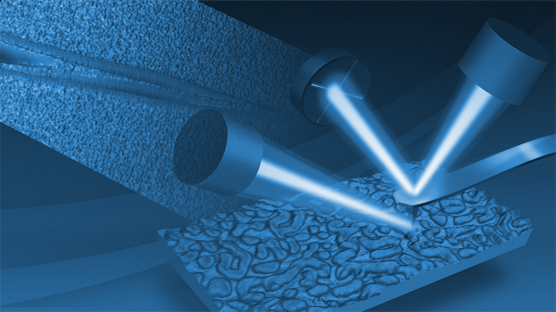
What NanoIR/AFM‑IR provides:
NanoIR combines AFM with a tunable infrared laser to deliver localized chemical information with nanoscale spatial resolution. By detecting the material’s response to infrared absorption, NanoIR enables chemical mapping without the thickness‑related artifacts common in conventional IR methods.
This technique is particularly valuable when chemistry — not just structure — drives performance differences.
Typical thin‑film questions nanoIR/AFM-IR answers:
- Are there chemical differences across domains or interfaces?
- Does local chemistry explain performance variation?
- How are components distributed within a thin film?
- Can chemistry be directly correlated with nanoscale structure or mechanics?
Common uses in thin films applications include:
(See all nanoIR spectroscopy resources for thin film characterization here)
About Our Nanomechanical Test Instruments
Best used when you need:
- Quantitative mechanical properties measured at the nanoscale
- Correlation of mechanical response with local structure or morphology
- Property mapping across heterogeneous or patterned thin films
- Insight into near‑surface or thin‑film behavior where bulk tests are not representative
What nanomechanical testing provides:
Nanomechanical testing enables localized measurement of mechanical properties such as hardness, elastic modulus, adhesion, and viscoelastic response at length scales relevant to thin films and interfaces. By controlling applied load and penetration depth, these techniques probe film behavior while minimizing substrate influence.
In thin‑film characterization workflows, nanoscale nanomechanical measurements are often used to correlate mechanical response with surface structure, morphology, or other nanoscale features identified by optical or scanning probe methods. Property mapping capabilities allow spatial variations in mechanical behavior to be resolved across films that appear uniform at larger scales.
Typical thin‑film questions nanomechanical testing answers:
- How do mechanical properties vary across the film surface or between features?
- Is local stiffness or hardness correlated with nanoscale structure or morphology?
- How does near‑surface mechanical behavior differ from bulk response?
- Are mechanical properties uniform across the film at the scale relevant to performance?
Common uses in thin films applications include:
(See all nanomechanical testing resources for thin film characterization here)
Performance, Wear, & Reliability Evaluation Technologies
Performance and reliability evaluation technologies are used to assess how thin films behave under load, contact, motion, or over time. These methods are commonly applied during qualification, failure analysis, and scale‑up to connect measured properties to real‑world operating conditions.
About Our Nanomechanical Test Instruments
Best used when you need:
- Mechanical property data tied directly to performance or reliability requirements
- Assessment of adhesion, fracture, or deformation behavior under load
- Insight into depth‑, time‑, or environmentally-dependent mechanical response
- Information about failure mechanisms that limit durability or lifetime
What nanomechanical testing provides:
Nanomechanical testing supports controlled loading and unloading of thin films to evaluate properties that govern performance and durability, including hardness, elastic modulus, adhesion strength, fracture behavior, and creep or viscoelastic response. By controlling load, penetration depth, and deformation mode, nanomechanical techniques connect measured properties directly to how a film performs under real mechanical stress.
In performance‑focused applications, nanomechanical data help connect measured properties to real‑world behavior under mechanical stress, processing conditions, or repeated loading. Depth‑dependent testing and dynamic methods provide insight into how films respond over time or under service‑relevant conditions.
Typical thin‑film questions nanomechanical testing answers:
- How do mechanical properties relate to durability or reliability?
- Does adhesion or fracture behavior limit performance or cause failure?
- Does the film fracture, creep, or wear under load?
- Does the film meet performance or reliability requirements?
Common uses in thin films applications include:
(See all nanomechanical testing resources for thin film characterization here)
About Our Tribometers & Mechanical Testers
Best used when you need:
- To evaluate durability under sliding, scratching, or fretting
- When wear and friction are system‑level concerns, not just material properties
- To solve real‑world field failures related to reliability or compatibility
- To rank coatings, lubricants, deposition methods, or material pairings by performance
What tribology/mechanical testing provides:
Tribology testing measures how thin films behave under controlled sliding contact by defining loads, motion, geometry, and environment. Outputs typically include wear depth or volume, coefficient of friction, and visual inspection of wear scars.
Just as importantly, tribology testing provides a structured workflow: define the problem first, identify the tribological system and dominant wear mode, then select or adapt a test — often guided by standards but tailored to the application. Matching laboratory wear modes to those observed in the field ensures that accelerated tests remain relevant.
Typical thin‑film questions tribology/mechanical testing answers:
- Under what loads, speeds, or distances does my coating survive?
- What wear mode is dominant — adhesive, cohesive, or abrasive?
- How does friction evolve during run‑in and steady‑state wear?
- Do lab tests reproduce field failure mechanisms?
- Which coating or material pairing delivers the best durability and lowest friction?
Common uses in thin films applications include:
(See all tribology/mechanical testing resources for thin film characterization here)
Choosing and Combining Techniques for Thin‑Film Characterization
No single technique tells the whole story. Each instrument is optimized for specific strengths—speed versus resolution, local detail versus large‑area context, intrinsic properties versus real‑world behavior. In practice, techniques are often layered: fast, non‑contact methods establish baseline uniformity; localized or nanoscale tools reveal structure, chemistry, or failure mechanisms; mechanical and tribological tests connect those findings to performance and durability. Used comparatively and in combination, these techniques validate one another and progressively build a more complete, confident understanding of thin film behavior.
The table below summarizes how common thin‑film characterization methods differ in what they measure, the role they play in a workflow, and how they are often combined. Use it to identify which techniques help answer your specific questions and see how they can be paired to increase confidence and reduce ambiguity.
FIND THE RIGHT TECHNOLOGY FOR YOUR MEASUREMENTS:
| Technique | Sample interaction | What it provides (including scale where relevant) | Typically used to assess | Questions commonly answered |
|---|---|---|---|---|
| 3D Optical Profilometry | Non‑contact optical – white‑light interferometry | Quantitative 3D surface maps providing step height, surface roughness, texture, and large‑area uniformity measurements from micron to millimeter length scales; up to full‑wafer via stitching | Topography, roughness, step height, and thickness (3D, non-contact) | Is the surface uniform across the sample? Where are roughness/step variations and localized anomalies? |
| Ellipsometry/Reflectometry | Non‑contact optical – multi‑angle reflectance | Film thickness, thickness uniformity, and optical constants (n, k), including multilayer optical response, obtained through model‑based analysis of reflected light; supports single‑point and wafer mapping depending on system | Thickness and optical constants | What is the film thickness and uniformity? What are the optical constants? How does a multilayer stack behave optically? |
| Stylus Profilometry | Contact – mechanical stylus scanning | Direct, trace‑based measurements of step height, film thickness, and surface texture along defined scan paths, providing high vertical resolution where physical contact is acceptable | Topography, roughness, step height, and thickness (2D, contact) | What is the actual step height or thickness at this location? Can I validate an optical result? |
| Atomic Force Microscopy (AFM) | Contact or tapping – localized tip-sample interaction with force feedback | Nanoscale surface topography and localized property contrast, enabling spatially resolved mapping of mechanical, electrical, or functional variations that are not visible at larger scales | Topography and mechanical, electrical properties and variation | What nanoscale features or heterogeneity exist? Why does behavior vary when larger‑scale measurements look uniform? |
| nanoIR (AFM‑IR) | Contact or tapping – AFM tip with infrared excitation | Nanoscale chemical identification and chemical distribution maps by combining AFM spatial resolution with infrared spectroscopy, enabling localized composition analysis below optical limits; sub‑micron to nanoscale | Chemical properties, composition, and variation | Are there local chemical differences in the film? Is chemistry driving adhesion, performance, or failure? |
| Nanomechanical Testing | Contact – localized normal and lateral loads | Quantitative mechanical response of thin films under applied load, including hardness, elastic modulus, deformation behavior, and indicators of adhesion or fracture that influence reliability | Mechanical response, adhesion, damage onset, and failure progression (nanoscale, localized) | How does the film respond under load? Are mechanical properties driving reliability risk? Is substrate influence affecting interpretation? |
| Tribology/Mechanical Testing | Contact – sliding and repeated mechanical interaction | Performance‑oriented measurements of friction, wear, adhesion failure, and durability under representative contact and sliding conditions, supporting evaluation of coating reliability in use | Performance and durability (macroscale, in-use, system-level) | How will the coating perform in use? What wear/failure mechanisms dominate? What limits durability and reliability? |
Contact A Bruker Thin Films Characterization Expert
Ask us a question, request more information, or get expert instrument and configuration recommendations to fit your specific measurement needs.