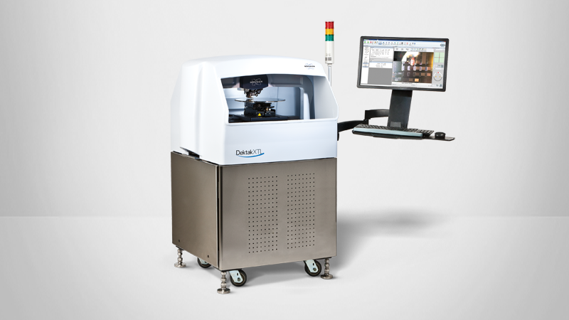
Dektak Stylus Profiler ー 第11世代触針式プロファイリングシステム
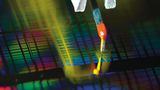
ブルカーのスタイラスプロファイラー”Dektakシリーズ”の特徴は、4Å以下という段差測定再現性を実現する革新的なデザインに表れています。この大きな進歩は、Dektakの50年以上に渡る技術革新と産業的なリーダーシップにより成し遂げられました。これまでの50年に渡るDektakの世界に 先駆ける技術を組み合わせることで、Dektak シリーズはR&DからQCにおけるプロセス開発の測定管理を可能にする究極の測定パフォーマンス、使いやすさ、測定機としての偉大なる価値を提供します。11世代に渡る科学技術のブレイクスルーを盛り込んだDektakシリーズは、マイクロエレクトロニクス、半導体、太陽光パネル、高輝度LED、医療系技術、有機向き材料科学分野において重要となるナノメートルレベルの表面形状測定を可能にします。
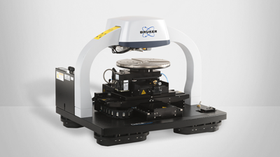
触針式プロファイリングシステム (触針式薄膜段差計)ラインナップ
究極の測定パフォーマンスへのステップアップ
ブルカー製スタイラスプロファイラ”DektakXT”の特徴は、4Å以下という段差測定再現性を実現する革新的なデザインに表れています。この大きな進歩は、Dektakの50年以上に渡る技術革新と産業的なリーダーシップにより成し遂げられました。これまでの50年に渡るDektakの世界に 先駆ける技術を組み合わせることで、DektakXTはR&DからQCにおけるプロセス開発の測定管理を可能にする究極の測定パフォーマンス、使いやすさ、測定機としての偉大なる価値を提供します。10世代に渡る科学技術のブレイクスルーを盛り込んだDektakXTは、マイクロエレクトロニクス、半導体、太陽光パネル、高輝度LED、医療系技術、有機向き材料科学分野において重要となるナノメートルレベルの表面形状測定を可能にします。
Frequently Asked Questions About Stylus Profilometry Technology
Stylus profilometers trace a low force, sharp tip across the surface to record height as a function of position. From that line trace, surface roughness, step height, waviness, and form can be calculated. Modern systems also support recipe based workflows for these measurements.
LEARN MORE:
Though the native measurement for stylus is a line profile, 3D maps are built by stitching multiple line traces across an area, providing areal visualization and statistics.
Stylus can be a good choice when sample surfaces are transparent or non-reflective surfaces, and when long scan lengths or large vertical ranges are needed. It is also often the most economical path to traceable roughness and step‑height metrology for growing labs. Optical methods often deliver faster 3D areal maps; AFM excels at ultra‑high lateral resolution over small fields of view.
LEARN MORE:
Stylus profilers are typically used to measure Ra, Rq, Rz, step height, waviness, and form. Parameters like Ra, Rq, and Rz come from the filtered profile, while step height, waviness, and form are computed from leveled, standardized traces. Proper cutoff selection and leveling are essential so results are comparable across sites and operators.
LEARN MORE:
For step height, typical vertical repeatability is on the order of a few angstroms to ~1 nm under controlled conditions, with sub‑nanometer repeatability possible on optimized setups and certified standards. Some key variables affecting accuracy and repeatability are tip condition/geometry, applied force, sample fixturing, vibration/thermal stability, and analysis procedures.
Typically, in fact our acceptance criteria is on a 100nm step height with 4 angstrom repeatability, which is about a .4% repeatability.
Benchtop systems can accommodate small coupons up to 8-inch full wafers, while production models (like DektakXTL) support up to 12-inch wafers and panels up to 350mm square; including encoded stages and multi‑site automation. Exact limits depend on the model, stage travel, and accessories.
Sample thickness can be up to 50mm. Geometries are typically flat. Wafers held down with vacuum chuck to limit contact of wafer surface.
LEARN MORE:
Lateral resolution is limited by tip radius, so choosing an appropriate tip is important. Steep slopes and narrow features can be misrepresented if the tip cannot access them fully. Very soft or tacky films may require minimal force and specific tips; in some cases, an optical profilometer may bebetter suited.
Dektak ウェビナーシリーズ
製品導入の検討や研究者の皆様の課題解決に直結する、最新のアプリケーション事例、測定モード、測定技術、分析手法のヒントやアイデアなど、様々なコンテンツを提供します。
Support

どのようなお手伝いが必要ですか?
ブルカーはお客様と協力し、実世界のアプリケーション課題を解決します。次世代技術を開発し、お客様が適切なシステムとアクセサリーを選択できるようサポートします。このパートナーシップは、機器販売後もトレーニングや延長サービスを通じて継続します。
高度な訓練を受けたサポートエンジニア、アプリケーションサイエンティスト、専門知識を持つエキスパートからなるチームが、システムサービスやアップグレード、アプリケーションサポート、トレーニングを通じて、お客様の生産性最大化に全力を尽くします。