先进的探针式轮廓仪
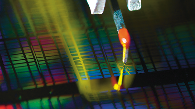
布鲁克的Dektak®探针式轮廓仪是五十多年专有技术进步的顶峰。它们提供可重复、可靠和准确的测量:从传统的台阶高度测量和二维粗糙度的表面表征到高级三维形貌和薄膜应力分析。Dektak 探针式轮廓仪已被广泛接受为薄膜厚度、应力、表面粗糙度和形貌测量的金标准,应用到从学术研究到半导体过程控制等不同领域。
找到最适合你的探针式轮廓仪
超过五十年的分析创新
Dektak 品牌拥有第一个用于薄膜测量的探查器、第一个基于微处理器的探查器、第一个具有 3D 功能的探查器、第一个基于 PC 的探查器以及第一个自动化的 300mm 探查器。现在,DektakXT 延续了这一开创性"第一"的传统,成为第一个实现单拱形设计的手写笔探查器,第一个集成了简单可靠的手写笔交换器,以及第一个利用 64 位并行处理架构实现最佳测量和运行效率的手写笔探查器。
Frequently Asked Questions About Stylus Profilometry Technology
Stylus profilometers trace a low force, sharp tip across the surface to record height as a function of position. From that line trace, surface roughness, step height, waviness, and form can be calculated. Modern systems also support recipe based workflows for these measurements.
LEARN MORE:
Though the native measurement for stylus is a line profile, 3D maps are built by stitching multiple line traces across an area, providing areal visualization and statistics.
Stylus can be a good choice when sample surfaces are transparent or non-reflective surfaces, and when long scan lengths or large vertical ranges are needed. It is also often the most economical path to traceable roughness and step‑height metrology for growing labs. Optical methods often deliver faster 3D areal maps; AFM excels at ultra‑high lateral resolution over small fields of view.
LEARN MORE:
Stylus profilers are typically used to measure Ra, Rq, Rz, step height, waviness, and form. Parameters like Ra, Rq, and Rz come from the filtered profile, while step height, waviness, and form are computed from leveled, standardized traces. Proper cutoff selection and leveling are essential so results are comparable across sites and operators.
LEARN MORE:
For step height, typical vertical repeatability is on the order of a few angstroms to ~1 nm under controlled conditions, with sub‑nanometer repeatability possible on optimized setups and certified standards. Some key variables affecting accuracy and repeatability are tip condition/geometry, applied force, sample fixturing, vibration/thermal stability, and analysis procedures.
Typically, in fact our acceptance criteria is on a 100nm step height with 4 angstrom repeatability, which is about a .4% repeatability.
Benchtop systems can accommodate small coupons up to 8-inch full wafers, while production models (like DektakXTL) support up to 12-inch wafers and panels up to 350mm square; including encoded stages and multi‑site automation. Exact limits depend on the model, stage travel, and accessories.
Sample thickness can be up to 50mm. Geometries are typically flat. Wafers held down with vacuum chuck to limit contact of wafer surface.
LEARN MORE:
Lateral resolution is limited by tip radius, so choosing an appropriate tip is important. Steep slopes and narrow features can be misrepresented if the tip cannot access them fully. Very soft or tacky films may require minimal force and specific tips; in some cases, an optical profilometer may bebetter suited.
Dektak探针式轮廓仪网络研讨会系列
我们的网络研讨会涵盖最佳实践,介绍新产品,为棘手的问题提供快速解决方案,并为新的应用程序、模式或技术提供想法。
支持

我们能提供哪些支持?
布鲁克致力于为客户解决实际应用问题。我们不断开发新的测试技术,并帮助客户选择最合适的系统与配件。我们通过培训或者延保等方式,与客户保持长久的合作关系。
我们拥有专业的服务团队,支持工程师、应用科学家和专家团队将通过系统服务,功能升级,应用拓展和技术培训等多种方式帮助您最大化的发挥设备的效能。