
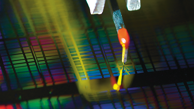
동급 최강의 스타일러스 프로파일러
브루커의 Dektak® 스타일러스 프로파일러는 50년 이상의 독점 기술의 산물입니다. 이 프로파일러는 기존의2D 조도 표면 특성화, 단차 측정, 고급 3D 매핑 및 박막 응력 분석 등 반복 가능하고 신뢰할 수 있으며 정확한 측정을 제공합니다. Dektak 표면 프로파일러는 학술 연구에서 반도체 공정 제어 등 다양한 응용 분야에서 박막 두께, 응력, 표면 조도와 형태 측정을 위한 표준으로 널리 인정받고 있습니다.
당신을 위한 최고의 덱탁 찾기

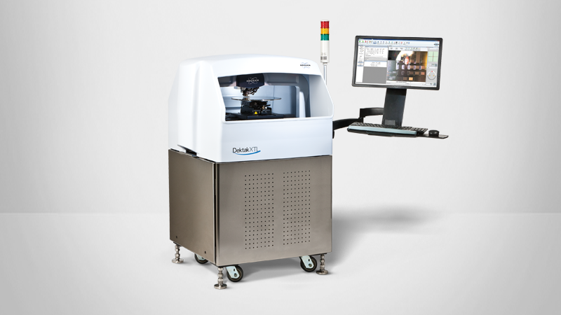
50년 이상 프로파일링 혁신
덱탁은 박막 측정을 위한 최초의 프로파일러, 최초의 마이크로프로세서 기반 프로파일러, 3D 기능을 갖춘 최초의 프로파일러, 최초의 PC 기반 프로파일러 및 최초의 자동화된 300mm 프로파일러를 자랑합니다. 현재 덱탁XT는 단일 아치형 설계를 구현한 최초의 스타일러스 프로파일러이며, 쉽고 안정적인 스타일러스 교환을 통합한 최초이자, 최적의 측정 및 작동 효율성을 달성하기 위해 64비트 병렬 처리 아키텍처를 활용하는 최초의 스타일러스 프로파일러로서 “firsts"를 개척해 왔습니다.
Frequently Asked Questions About Stylus Profilometry Technology
Stylus profilometers trace a low force, sharp tip across the surface to record height as a function of position. From that line trace, surface roughness, step height, waviness, and form can be calculated. Modern systems also support recipe based workflows for these measurements.
LEARN MORE:
Stylus profilers are typically used to measure Ra, Rq, Rz, step height, waviness, and form. Parameters like Ra, Rq, and Rz come from the filtered profile, while step height, waviness, and form are computed from leveled, standardized traces. Proper cutoff selection and leveling are essential so results are comparable across sites and operators.
LEARN MORE:
A stylus force of 1 mg combined with a 2 µm stylus tip will not cause any damage on the majority of surface materials. Sharper styli and very soft materials will require lower stylus forces to avoid scratches. Alternatively a greater stylus radius of up to 25 µm may be used on delicate materials.
Though the native measurement for stylus is a line profile, 3D maps are built by stitching multiple line traces across an area, providing areal visualization and statistics.
Stylus can be a good choice when sample surfaces are transparent or non-reflective surfaces, and when long scan lengths or large vertical ranges are needed. It is also often the most economical path to traceable roughness and step‑height metrology for growing labs. Optical methods often deliver faster 3D areal maps; AFM excels at ultra‑high lateral resolution over small fields of view.
LEARN MORE:
More About Bruker's Dektak Stylus Profiler Systems
The sample is placed on a slider that slides over a highly polished flat glass block. The surface profile is measured by drawing the sample slider at constant speed underneath the stylus tip.
The vertical movement of the stylus tip is measured using LVDT (Linear Variable Differential Transformer) technology, which converts the stylus displacement into a highly precise and linear electrical signal.
Benchtop systems can accommodate small coupons up to full 8” wafers, while production models support large wafers and panels up to 12” size with encoded stages and multi‑site automation. The maximum sample height is 50 mm. Exact limits depend on the model, stage travel, and accessories.
For step height, typical vertical repeatability is on the order of a few angstroms to ~1 nm under controlled conditions, with sub‑nanometer repeatability possible on optimized setups and certified standards. Some key variables affecting accuracy and repeatability are tip condition/geometry, applied force, sample fixturing, vibration/thermal stability, and analysis procedures.
The standard stylus force of a Dektak stylus profiler ranges from 1 to 15 mg. For very delicate materials the force range can be extended downward to 0.03 mg (N-Lite force range).
The Dektak diamond stylus tips have a cono-spherical shape with radii ranging from 25 µm down to very sharp 50 nm. Often, Dektak stylus profilers are equipped with a stylus tip with 2 µm radius which is the recommended stylus radius for roughness measurements.
Sharper styli may be used if higher lateral resolution is required, while styli with greater radii may be useful on very sensitive surfaces.
Dektak styli are easily exchanged within a minute with the included stylus exchange tool. No tiny screwdrivers, Allen wrenches, or tweezers needed. No recalibration needed: Stylus exchange does not affect the calibration of the vertical scale, force scale or optical view.
Every Dektak stylus profiler supports recipe-based workflows for measurement and data analysis. In addition to measurement and automated analysis, Dektak recipes support the acquisition of sample information (e.g., wafer ID and part number), automatic saving of data files using template-generated filenames, and reporting of analysis results (e.g., step heights and roughness) to database tables.
Dektak stylus profilers with motorized XY-stage also allow to generate and run multi-site automation recipes, complete with wafer registration with alignment features (manual or by optical pattern recognition) and automated analysis and database reporting.
Selecting and Upgrading a Dektak Stylus Profiler
- The sub-nm vertical resolution of the LVDT (Linear Variable Differential Transformer) height sensor enables the measurement of heights, depths, and roughness down to single-nanometer levels and below.
- The LVDT sensor technology provides a large vertical range (up to 1 mm) and at the same time very low stylus forces (down to 0.03 mg) with a single sensor head.
- The vertical scale calibration shows excellent long-term stability.
- Moving the sample over a polished flat glass block provides a reference surface that is flat within a few nanometers over the full scan length of 55 mm.
- Dektak styli can be easily exchanged using the included stylus exchange tool without a need for recalibration of vertical range or stylus force.
Lateral resolution is limited by tip radius, so choosing an appropriate tip is important. Steep slopes and narrow features can be misrepresented if the tip cannot access them fully. Very soft or tacky films may require minimal force and specific tips; in some cases, an optical profilometer may bebetter suited.
Bruker provides applications consulting, troubleshooting, and best practice guidance, along with optional service plans for ongoing support, maintenance, and training.
Contact us to arrange a demonstration or submit samples for an evaluation tailored to your test geometry and materials.
Bruker offers upgrade options for users of legacy Dektak systems. Contact us to discuss your current system, measurement requirements, and available options for moving to a current Dektak platform.
덱탁 웨비나 시리즈
당사의 웨비나는 모범 사례를 다루고, 신제품을 소개하고, 까다로운 질문에 대한 빠른 솔루션을 제공하고, 새로운 애플리케이션, 모드 또는 기술에 대한 아이디어를 제공합니다.
어떻게 도와드릴까요?

Bruker는 고객과 협력하여 실제 애플리케이션 이슈를 해결합니다. 당사는 차세대 기술을 개발하고 고객이 적합한 시스템 및 액세서리를 선택할 수 있도록 지원합니다. 이러한 협력은 장비가 판매된 후에도 오랫동안 교육 및 확장 서비스를 통해 계속됩니다.
고도로 훈련된 지원 엔지니어, 애플리케이션 과학자 및 주제 전문가 팀은 시스템 서비스 및 업그레이드뿐만 아니라 애플리케이션 지원 및 교육을 통해 생산성을 극대화하기위해 전적으로 최선을 다하고 있습니다.