
덱탁XTL
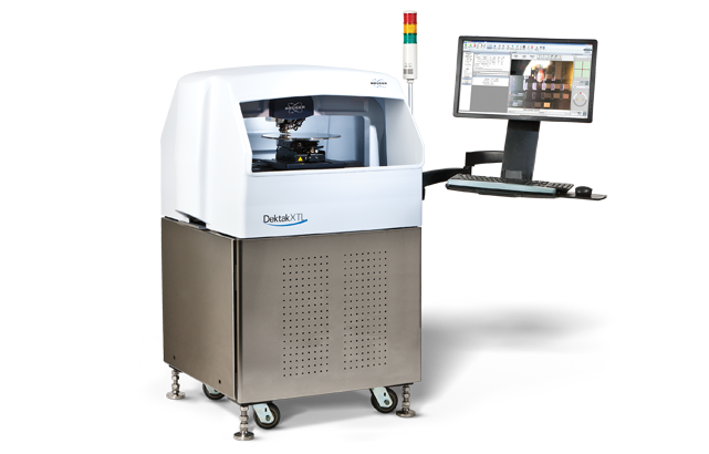
덱탁 XTL
덱탁 XTL™ 스타일러스 프로파일러는 최대 350mm x 350mm크기의 시료를 계측할 수 있으며, 대형 웨이퍼 및 패널 제조에 대해 고성능의 반복성과 재현성을 제공합니다. 덱탁XTL은 공압 진동 차단 기능과 쉽게 접근할 수 있는 연동 도어가 있는 완전히 밀폐된 워크 스테이션의 특징을 갖추고 있어 최신 기술을 바탕으로 한 까다로운 생산 현장 환경에 이상적입니다. 듀얼 카메라 아키텍처는 개선된 공간 인식을 가능하게 하여, 높은 수준의 자동화로 제조 처리량을 극대화합니다.
업계 최고의 자동화 및 분석 소프트웨어
향상된 소프트웨어 기능을 통해 덱탁 XTL을 가장 강력하고 사용하기 쉬운 스타일러스 프로파일러로 만듭니다. 이 시스템은 무제한 측정 사이트, 3D 매핑 및 수백 개의 내장된 분석 도구를 사용하여 고도로 맞춤화된 특성화를 가능하게 하는 Vision64 소프트웨어를 사용합니다. Vision Microform소프트웨어는 곡률 반경과 같은 모양을 측정합니다. 패턴 인식은 작업자 오류를 최소화하고 측정 위치 정확도를 향상시킵니다. all-in-one 소프트웨어 패키지는 데이터 수집 및 분석을 직관적인 워크플로우와 결합합니다.

타의 추종을 불허하는 스타일러스 기술

덱탁 XTL은 50 년 이상의 스타일러스 전문 지식과 생산 시설에 대한 응용분야 맞춤화를 기반으로 현재와 미래의 엄격한 업계 로드맵을 모두 충족합니다. 300mm의 고정밀 인코딩된 XY 스테이징은 엄격한 gage R&R 요구 사항을 충족할 수 있는 신뢰할 수 있는 도구를 제조업체에 제공합니다. 고 배율 듀얼 뷰 카메라가 탑재된 덱탁의 듀얼 카메라 컨트롤은 향상된 공간 인지도를 제공합니다. 실시간 비디오에서 포인트 앤 클릭 위치 지정을 통해 작업자는 빠르고 쉬운 측정 설정 및 자동화 프로그래밍을 위해 샘플을 적절한 위치에 신속하게 배치할 수 있습니다. 시스템의 대형 연동 도어는 샘플 로딩/언로딩을 위해 안전하고 쉽게 접근할 수 있도록 해 줍니다.
다른 하드웨어 기능은 다음과 같습니다.
- 업계 최고의 성능을 위한 단일 아치형 아키텍처 및 통합 진동 차단
- 신속한 변경 self-정렬 스타일러스
- 더 빠른 자동화된 데이터 수집을 위한 고정밀 인코딩된 XY 단계
- 소프트 터치 기술과 1mm 측정 범위가 있는 N-Lite 저력을 동시에 사용하여 섬세하고 수직적인 범위 샘플 측정
Frequently Asked Questions
Dektak XTL is designed for large-format and production-oriented measurements. It combines a motorized, high-accuracy encoded 300 mm XY stage, continuous 360° theta positioning, an enclosed workstation, integrated vibration isolation, and automation capabilities for process development and QA/QC environments.
Dektak XTL accommodates wafers up to 300 mm and samples up to 350 mm × 350 mm, with a maximum sample thickness of 50 mm. This supports both large wafers and panel or other large-substrate applications.
Dektak XTL uses dual-camera viewing with top and high-magnification side views. Operators can easily navigate to points of interest, orient the sample, and define scan start and end positions directly from the live video.
The encoded 300 mm XY stage and continuous theta positioning support automated measurements at unlimited measurement sites. Operators can program fiducials and measurement sites, while pattern recognition can improve measurement-location accuracy and reduce operator-to-operator variability. Measurement results can also be automatically analyzed and logged to a database.
Common applications include semiconductor wafers, touch panels, flat-panel displays, solar coatings, printed circuit boards, and flexible electronics. Measurements include deposited-film and resist step height, etch-rate determination, CMP erosion and dishing, coating thickness, and printed circuit board bumps and step heights.
You can request a quote using our online form, or contact us directly.
More About Bruker's Dektak Stylus Profiler Systems
The sample is placed on a slider that slides over a highly polished flat glass block. The surface profile is measured by drawing the sample slider at constant speed underneath the stylus tip.
The vertical movement of the stylus tip is measured using LVDT (Linear Variable Differential Transformer) technology, which converts the stylus displacement into a highly precise and linear electrical signal.
Benchtop systems can accommodate small coupons up to full 8” wafers, while production models support large wafers and panels up to 12” size with encoded stages and multi‑site automation. The maximum sample height is 50 mm. Exact limits depend on the model, stage travel, and accessories.
For step height, typical vertical repeatability is on the order of a few angstroms to ~1 nm under controlled conditions, with sub‑nanometer repeatability possible on optimized setups and certified standards. Some key variables affecting accuracy and repeatability are tip condition/geometry, applied force, sample fixturing, vibration/thermal stability, and analysis procedures.
The standard stylus force of a Dektak stylus profiler ranges from 1 to 15 mg. For very delicate materials the force range can be extended downward to 0.03 mg (N-Lite force range).
The Dektak diamond stylus tips have a cono-spherical shape with radii ranging from 25 µm down to very sharp 50 nm. Often, Dektak stylus profilers are equipped with a stylus tip with 2 µm radius which is the recommended stylus radius for roughness measurements.
Sharper styli may be used if higher lateral resolution is required, while styli with greater radii may be useful on very sensitive surfaces.
Dektak styli are easily exchanged within a minute with the included stylus exchange tool. No tiny screwdrivers, Allen wrenches, or tweezers needed. No recalibration needed: Stylus exchange does not affect the calibration of the vertical scale, force scale or optical view.
Every Dektak stylus profiler supports recipe-based workflows for measurement and data analysis. In addition to measurement and automated analysis, Dektak recipes support the acquisition of sample information (e.g., wafer ID and part number), automatic saving of data files using template-generated filenames, and reporting of analysis results (e.g., step heights and roughness) to database tables.
Dektak stylus profilers with motorized XY-stage also allow to generate and run multi-site automation recipes, complete with wafer registration with alignment features (manual or by optical pattern recognition) and automated analysis and database reporting.
Selecting and Upgrading a Dektak Stylus Profiler
- The sub-nm vertical resolution of the LVDT (Linear Variable Differential Transformer) height sensor enables the measurement of heights, depths, and roughness down to single-nanometer levels and below.
- The LVDT sensor technology provides a large vertical range (up to 1 mm) and at the same time very low stylus forces (down to 0.03 mg) with a single sensor head.
- The vertical scale calibration shows excellent long-term stability.
- Moving the sample over a polished flat glass block provides a reference surface that is flat within a few nanometers over the full scan length of 55 mm.
- Dektak styli can be easily exchanged using the included stylus exchange tool without a need for recalibration of vertical range or stylus force.
Lateral resolution is limited by tip radius, so choosing an appropriate tip is important. Steep slopes and narrow features can be misrepresented if the tip cannot access them fully. Very soft or tacky films may require minimal force and specific tips; in some cases, an optical profilometer may bebetter suited.
Bruker provides applications consulting, troubleshooting, and best practice guidance, along with optional service plans for ongoing support, maintenance, and training.
Contact us to arrange a demonstration or submit samples for an evaluation tailored to your test geometry and materials.
Bruker offers upgrade options for users of legacy Dektak systems. Contact us to discuss your current system, measurement requirements, and available options for moving to a current Dektak platform.